Complementary metal-oxide-semiconductor image sensor and manufacturing method thereof

a technology of metal-oxidesemiconductor and image sensor, which is applied in the direction of diodes, semiconductor devices, radiation controlled devices, etc., can solve the problems of high adverse impact on signal transmission, so as to avoid metal contamination, improve signal transmission, and reduce contact resistance in the pixel region

Active Publication Date: 2017-01-03
UNITED MICROELECTRONICS CORP
View PDF125 Cites 7 Cited by
  • Summary
  • Abstract
  • Description
  • Claims
  • Application Information

AI Technical Summary

Benefits of technology

[0009]According to the manufacturing method of the semiconductor device provide by the present invention, the conductive bodies having a top surface higher than the substrate are formed in the pixel region, and the salicide layers are formed on the conductive bodies. Therefore, the salicide layer is formed away from the substrate, which includes the photosensitive elements. Consequently, metal contamination is avoided in the pixel region. More important, since salicide layers are allowed in the pixel region, contact resistances in the pixel region is efficaciously reduced and thus signal transmission is improved. Briefly speaking, the manufacturing method of semiconductor devices provided by the present invention is to form salicide layer, which is able to improve electrical performance of the CMOS image sensor, in the pixel region without causing metal contamination in the photosensitive element and increasing process complexity.

Problems solved by technology

However, it results that the pixel region suffers high contact resistances and signal transmission is adversely impacted.

Method used


Image

  • Complementary metal-oxide-semiconductor image sensor and manufacturing method thereof
  • Complementary metal-oxide-semiconductor image sensor and manufacturing method thereof
  • Complementary metal-oxide-semiconductor image sensor and manufacturing method thereof

Examples


Embodiment Construction

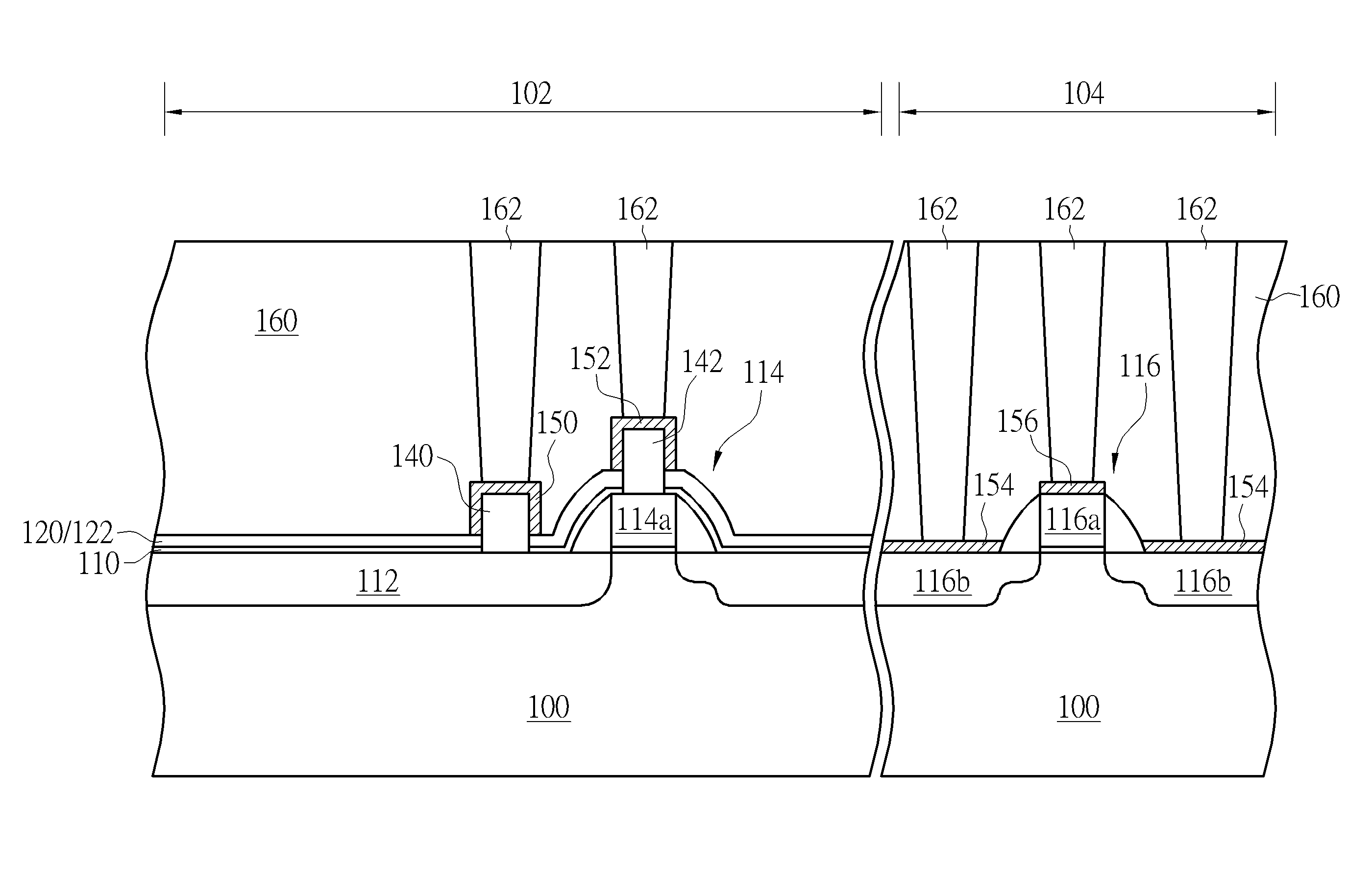
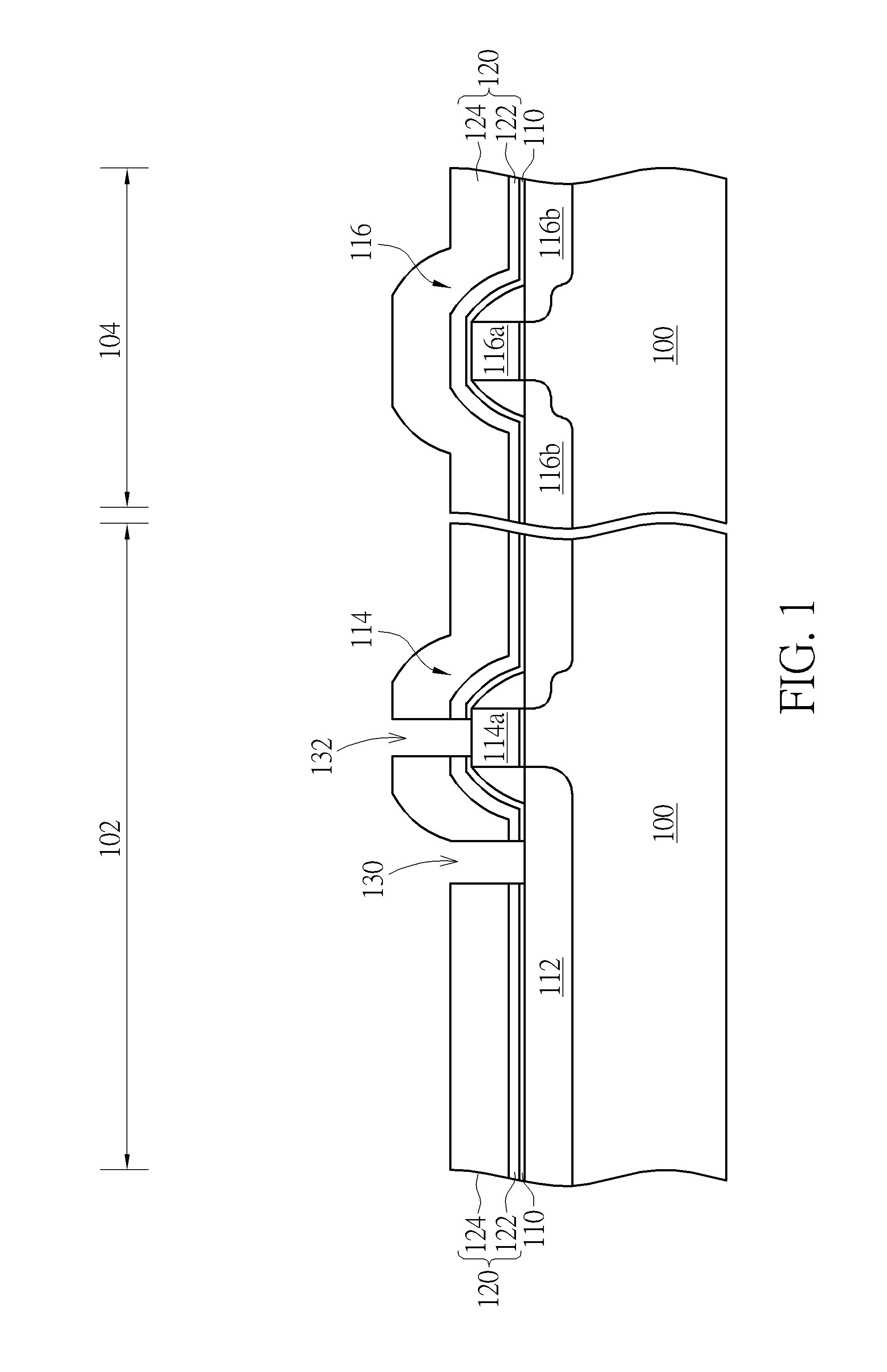
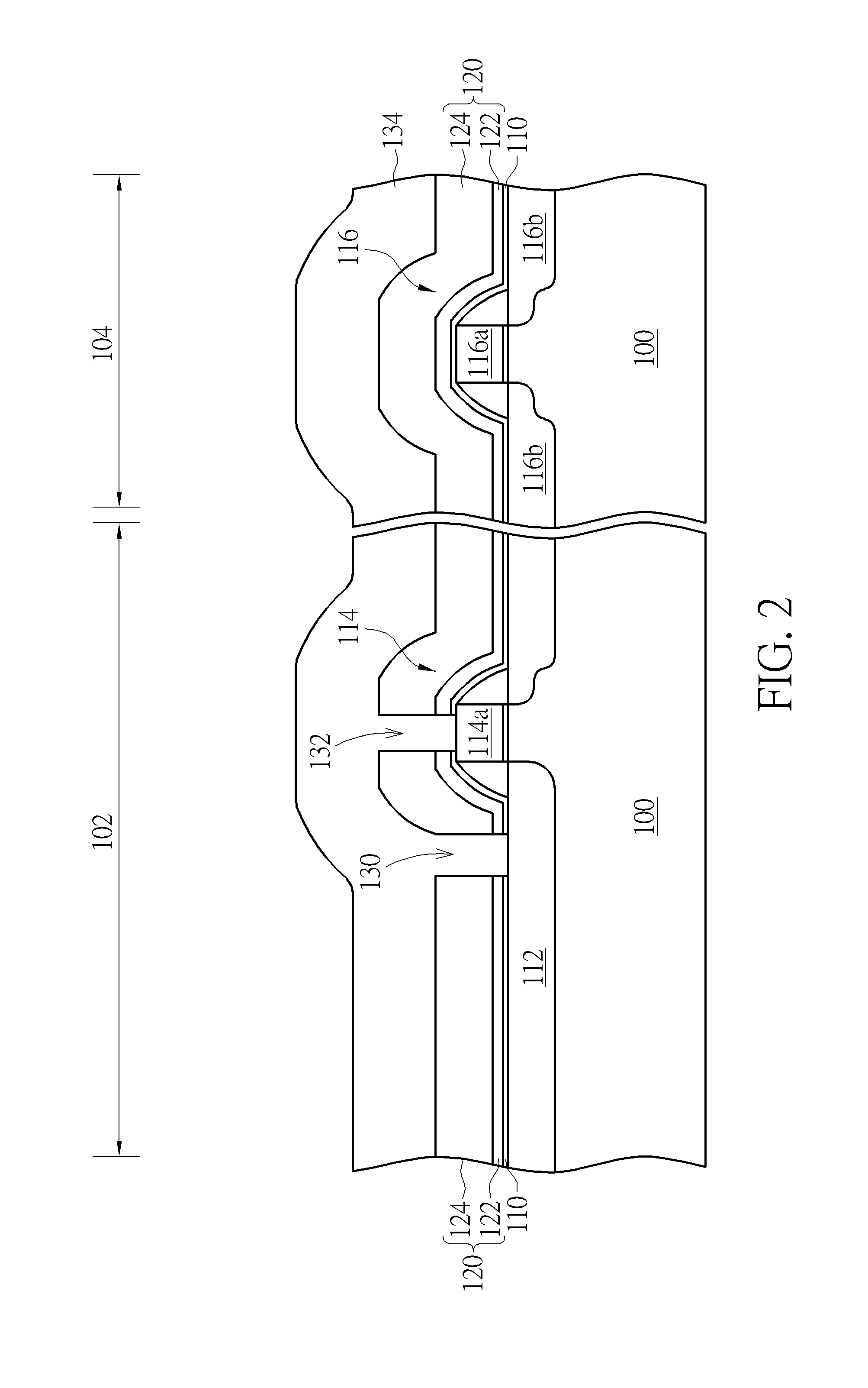
[0022]Please refer to FIGS. 1-7, which are schematic drawings illustrating a manufacturing method of a semiconductor device provided by a first preferred embodiment of the present invention. As shown in FIG. 1, a substrate 100 is provided. The substrate 100 can be a silicon substrate or other suitable semiconductor substrate. A plurality of isolation structures such as shallow trench isolations (not shown) is formed in the substrate 100 for defining a pixel region 102 and a periphery region 104 on the substrate 100. A plurality of photosensitive elements 112 and at least a first transistor 114 are formed in the pixel region 102. Logic elements are formed in the periphery region 104. For example but not limited to, at least a second transistor 116 is formed in the periphery region 104.

[0023]Please refer to FIG. 1 again. Next, a protecting layer 110 and a blocking layer 120 are sequentially formed on the substrate 100. In the preferred embodiment, the protecting layer 110 is an option...


PUM


Abstract

A method for manufacturing semiconductor devices includes following steps. A substrate having a pixel region and a periphery region defined thereon is provided, and at least a transistor is formed in the pixel region. A blocking layer is formed on the substrate, and the blocking layer includes a first opening exposing a portion of the substrate in the pixel region and a second opening exposing a portion of the transistor. A first conductive body is formed in the first opening and a second conductive body is formed in the second opening, respectively. The first conductive body protrudes from the substrate and the second conductive body protrudes from the transistor. A portion of the blocking layer is removed. A first salicide layer is formed on the first conductive body and a second salicide layer is formed on the second conductive body, respectively.

Description

BACKGROUND OF THE INVENTION[0001]1. Field of the Invention[0002]The present invention relates to a semiconductor device and a manufacturing method thereof, and more particularly, to the semiconductor device and the manufacturing method thereof for a complementary metal oxide semiconductor (herein abbreviated as CMOS) image sensor.[0003]2. Description of the Prior Art[0004]As the development of electronic products such as digital cameras and scanners progresses, the demand for image sensors increases accordingly. In general, image sensors in common usage nowadays are divided into two main categories: charge coupled device (CCD) sensors and CMOS image sensors (CIS). Primarily, CMOS image sensors have certain advantages of low operating voltage, low power consumption, and ability for random access. Furthermore, CMOS image sensors are currently capable of integration with the semiconductor fabrication process. Based on those benefits, the application of CMOS image sensors has increased ...

Claims


Application Information

Patent Timeline
Patent Type & Authority Patents(United States)
IPC IPC(8): H01L31/18H01L27/146
CPCH01L31/1804H01L27/14609H01L27/14643H01L27/14689H01L27/1463H01L27/14636
Inventor KAO, CHING-HUNG
Owner UNITED MICROELECTRONICS CORP
Why Eureka
Try Eureka