Thin film transistor array substrate
a technology of thin film transistors and array substrates, applied in the direction of electrical equipment, semiconductor devices, instruments, etc., can solve the problems of double damage to the drain electrode surface, increase in contact resistance between the pixel electrode and the drain electrode, etc., and achieve stable contact resistance and reduce the effect of step load
- Summary
- Abstract
- Description
- Claims
- Application Information
AI Technical Summary
Benefits of technology
Problems solved by technology
Method used
Image

Examples
first preferred embodiment
[0076]Preferred embodiments of the present invention will be described. The preferred embodiments described below are examples, and the application of the present invention is not limited to them. Further, like members in the drawings are denoted by like symbols, and overlapped description is suitably omitted.
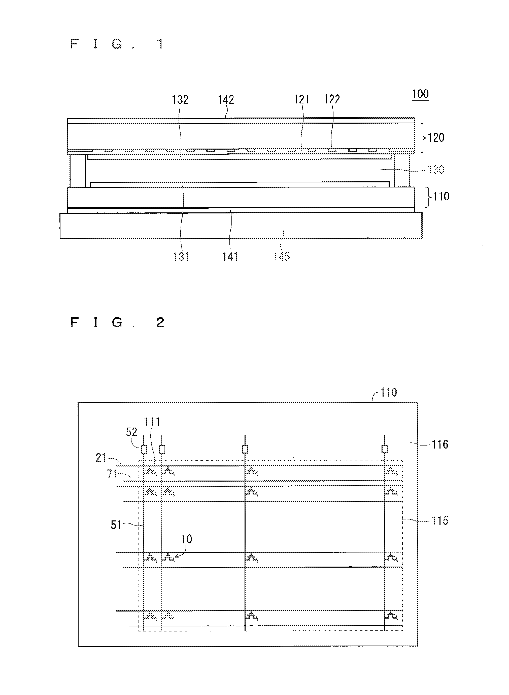
[0077]FIG. 1 is a cross sectional view illustrating a configuration of a liquid crystal display device 100 according to the first preferred embodiment. The liquid crystal display device 100 includes a liquid crystal display panel that has a structure where an array substrate 110 and a counter substrate 120 are arranged so as to be opposed to each other and a liquid crystal layer 130 is held therebetween. The counter substrate 120 that is arranged on a front surface side (visible side) of the liquid crystal display panel is, for example, a color filter substrate having a color filter 121 and a black matrix (BM) 122. Further, the array substrate 110 that is arranged on a rear sur...
second preferred embodiment
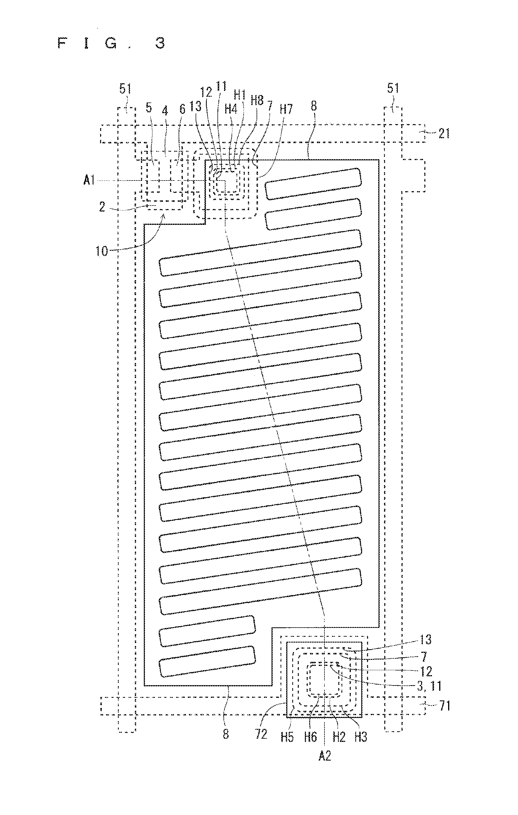
[0153]FIG. 29 and FIG. 30 are diagrams illustrating a configuration of an array substrate 110 according to the second preferred embodiment. FIG. 29 is the diagram illustrating a plan configuration of the pixels 111 in the array substrate 110. FIG. 30 is the diagram illustrating a cross-sectional configuration of the forming region (pixel region) for the pixels 111 and corresponds to a cross section taken along line B1-B2 shown in FIG. 29. Since configurations of a forming region (a wiring converting region) for a wiring converter 52 that connects a lead-out wiring 55 of a source wiring 51 with a lead-out wiring 25 on the same layer as a gate wiring 21 and a forming region (a terminal region) for terminals to be provided with end portions of the gate wirings 21 or the source wirings 51 are similar to those in the first preferred embodiment, illustration and description about them are omitted.
[0154]In the first preferred embodiment, an aperture H1 of a second interlayer insulating fil...
third preferred embodiment
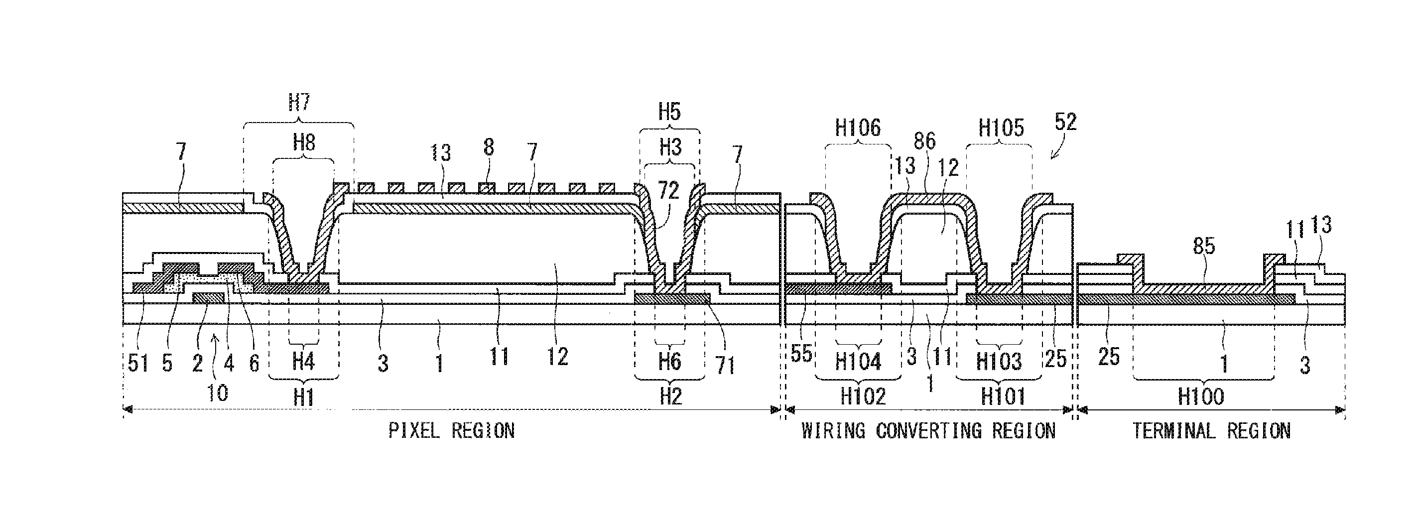
[0180]FIG. 41 and FIG. 42 are diagrams illustrating a configuration of an array substrate 110 according to the third preferred embodiment. FIG. 41 is a diagram illustrating a plan configuration of a pixel 111 in the array substrate 110. FIG. 42 is a diagram illustrating a cross-sectional configuration of a forming region (pixel region) for the pixels 111, and a forming region (a wiring converting region) for a wiring converter 52 for connecting a lead-out wiring 55 of a source wiring 51 with a lead-out wiring 25 on the same layer as a gate wiring 21. The cross section of the pixel region shown in FIG. 42 corresponds to a cross section taken along line B1-B2 shown in FIG. 41. Since a configuration of the forming region (a terminal region) provided with the end portion of the gate wiring 21 or the source wiring 51 is similar to that in the first preferred embodiment, illustration and description thereof are omitted.
[0181]In the second preferred embodiment, an aperture H7 of a common e...
PUM
| Property | Measurement | Unit |
|---|---|---|
| thickness | aaaaa | aaaaa |
| thickness | aaaaa | aaaaa |
| thickness | aaaaa | aaaaa |
Abstract
Description
Claims
Application Information
 - R&D
- Intellectual Property
- Life Sciences
- Materials
- Tech Scout
- Unparalleled Data Quality
- Higher Quality Content
- 60% Fewer Hallucinations
Browse by: Latest US Patents, China's latest patents, Technical Efficacy Thesaurus, Application Domain, Technology Topic, Popular Technical Reports.
© 2025 PatSnap. All rights reserved.Legal|Privacy policy|Modern Slavery Act Transparency Statement|Sitemap|About US| Contact US: help@patsnap.com