Non-contact probe measurement test bed for millimeter wave and terahertz circuits, integrated devices/components, systems for spectroscopy using sub-wavelength-size-samples

a technology of terahertz circuits and non-contact probes, which is applied in the direction of optical radiation measurement, instruments, material analysis, etc., can solve the problems of inconvenient use of probes, focal plane array antennas featuring very small details, and inability to directly contact probes for input impedance characterization

Active Publication Date: 2015-04-16
OHIO STATE INNOVATION FOUND
View PDF4 Cites 17 Cited by
  • Summary
  • Abstract
  • Description
  • Claims
  • Application Information

AI Technical Summary

Problems solved by technology

However, for the sub-millimeter or THz bands such probes are not readily available.
For example, focal plane array antennas feature very small details that do not allow direct probe contact for input impedance characterization.

Method used


Image

  • Non-contact probe measurement test bed for millimeter wave and terahertz circuits, integrated devices/components, systems for spectroscopy using sub-wavelength-size-samples
  • Non-contact probe measurement test bed for millimeter wave and terahertz circuits, integrated devices/components, systems for spectroscopy using sub-wavelength-size-samples
  • Non-contact probe measurement test bed for millimeter wave and terahertz circuits, integrated devices/components, systems for spectroscopy using sub-wavelength-size-samples

Examples


Embodiment Construction

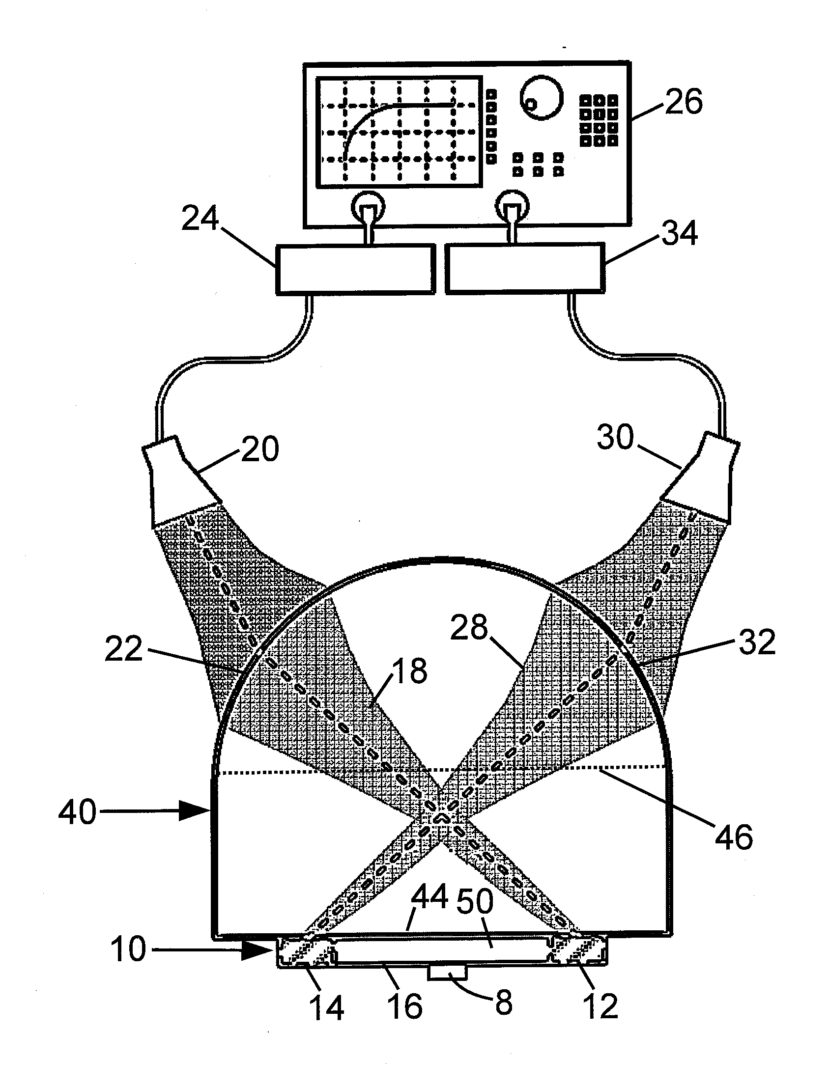
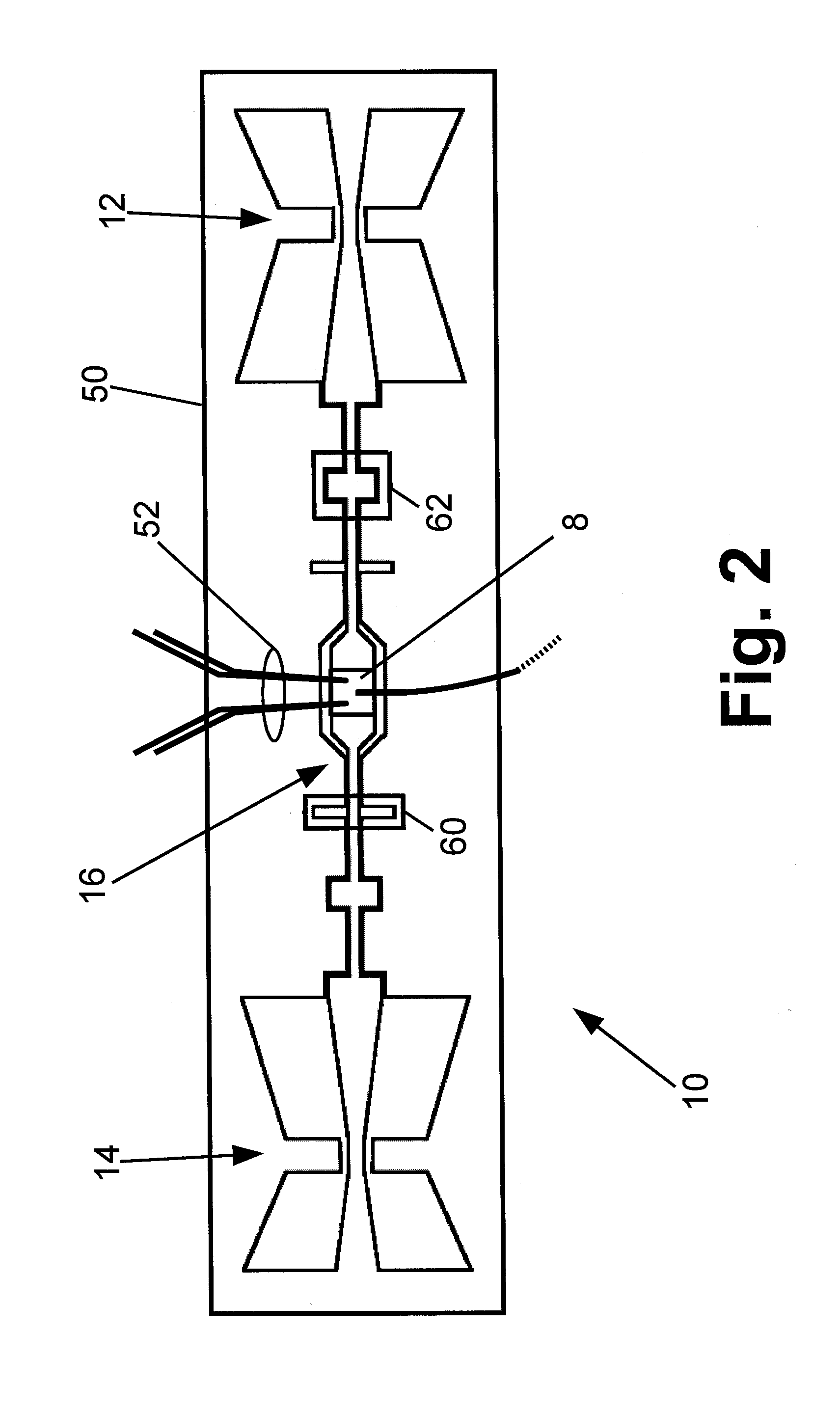
[0018]Disclosed herein are test beds and testing techniques for device and circuit testing at THz and mmW frequencies without the need to make electrical contact to convey electromagnetic signals. In some embodiments, the disclosed non-contact probe design includes beam-tilted THz and / or mmW antennas integrated into the coplanar environment of monolithic circuits and devices, such as high-speed transistors, diodes and integrated circuits. In some illustrative embodiments, a commercially available THz and / or mmW vector network analyzer (VNA) (with extension modules) and waveguide-fed horn antennas are used to excite the beam-tilted planar THz and / or mmW antennas integrated into the test device feed lines. In some embodiments, an extended hemispherical lens configuration is used to enhance THz and / or mmW coupling efficiency. Propagation effects and the antenna coupling artifacts are optionally removed using a conventional calibration method using several known loads (for example, a st...


PUM

PropertyMeasurementUnit
frequencyaaaaaaaaaa
wavelength rangeaaaaaaaaaa

Abstract

A test fixture for characterizing a device-under-test (DUT) includes first and second planar antennas and a planar waveguide arranged to guide terahertz (THz) and / or millimeter wave (mmW) radiation between the first and second planar antennas. The planar waveguide is further configured to couple THz and / or mmW radiation guided between the first and second planar antennas with the DUT. A beam forming apparatus is arranged to transmit a probe THz and / or mmW radiation beam to the first planar antenna of the test fixture. An electronic analyzer is configured to wirelessly receive a THz and / or mmW signal emitted by the second planar antenna responsive to transmission of the probe THz and / or mmW radiation beam to the first planar antenna. The planar antennas may be asymmetrical beam-tilted slot antennas.

Description

[0001]This application claims the benefit of U.S. Provisional Application No. 61 / 836,954 filed Jun. 19, 2013. U.S. Provisional Application No. 61 / 836,954 filed Jun. 19, 2013 is incorporated by reference herein in its entirety.[0002]This invention was made with Government support under Office of Naval Research Multidisciplinary University Research Initiative (ONR MURI) grant / contract no. N00014-11-1-0077, awarded by the Office of Naval Research (ONR). The government has certain rights in the invention.BACKGROUND[0003]The following relates to the millimeter or submillimeter, or equivalently extremely high frequency (EHF) to terahertz (THz), device characterization arts, millimeter to submillimeter (EHF to THz) device spectroscopy arts, millimeter or submillimeter (EHF or THz) device probe arts, and the like.[0004]The International Telecommunication Union (ITU) designates the frequency range 0.3 THz to 3 THz (where 1 THz=1012 Hz) as terahertz radiation, terahertz waves, or tremendously...

Claims


Application Information

Patent Timeline
Patent Type & Authority Applications(United States)
IPC IPC(8): G01N21/35G01R31/28
CPCG01N21/35G01R31/2832G01N21/3581G01R31/2822
Inventor SERTEL, KUBILAYCAGLAYAN, COSANTRICHOPOULOS, GEORGIOS
Owner OHIO STATE INNOVATION FOUND
Why Eureka
Try Eureka