Organic light emitting device and method of fabricating the same

a light emitting device and organic technology, applied in the direction of transistors, solid-state devices, thermoelectric devices, etc., can solve the problems of limiting the use of oxide thin film transistors in driving display devices, affecting the reliability of driving tfts, and affecting display performance. , to achieve the effect of efficient improvement of display performance and reliability

Active Publication Date: 2015-04-16
LG DISPLAY CO LTD
View PDF6 Cites 22 Cited by
  • Summary
  • Abstract
  • Description
  • Claims
  • Application Information

AI Technical Summary

Benefits of technology

[0010]An object of the disclosure is to provide an organic light emitting device including a hydrogen capturing material that is capable of efficiently improving reliability of a driving TFT and display performance.

Problems solved by technology

In the case that the organic light emitting device is driven by an oxide thin film transistor (TFT), if a characteristic of the oxide is changed due to various factors, a change in electric behavior of the transistor may cause a threshold voltage shift.
If the extent of the threshold voltage shift is outside a compensation range for a circuit driving an organic light emitting panel, the threshold voltage shift may result in a stain or a deviation of luminance that may be visible on the screen.
Accordingly, the threshold voltage shift may be an important factor causing degradation of the organic light emitting display device, and may limit use of the oxide thin film transistor in driving the display device.

Method used


Image

  • Organic light emitting device and method of fabricating the same
  • Organic light emitting device and method of fabricating the same
  • Organic light emitting device and method of fabricating the same

Examples


second embodiment

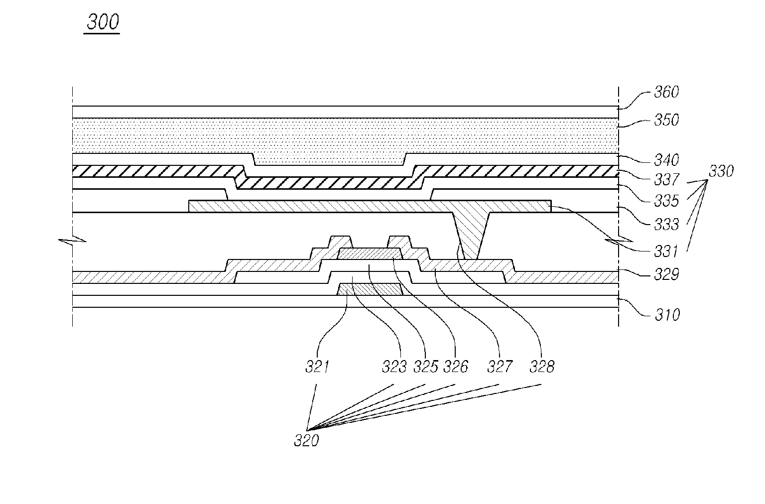
[0061]Referring to FIG. 3, an organic light emitting device 300 includes an oxide thin film transistor 320 arranged on the first substrate 310 in which a pixel region is defined, an organic light emitting diode 330 formed on the oxide thin film transistor 320, a passivation layer 340 formed on the organic light emitting diode 330, an adhesive layer 350 formed on the passivation layer 340, and a second substrate 360 formed on the adhesive layer 350.

[0062]The oxide thin film transistor 320 is formed on the first substrate 310. The oxide thin film transistor 320 includes a gate electrode 321, a gate insulation layer 323 formed on the gate electrode 321 to cover the first substrate 310, an active layer 325 formed of an oxide on the gate insulation layer 323, a source / drain electrode 327 formed on the active layer 325 and connected to the first electrode 331, and an etch stopper 326 formed between the source electrode and the drain electrode 327 on the active layer 325.

[0063]The first s...

third embodiment

[0168]Referring to FIG. 10, an organic light emitting device 1000 includes an oxide thin film transistor 1020 arranged on the first substrate 1010 in which a pixel region is defined, an organic light emitting diode 1030 formed on the oxide thin film transistor 1020 and corresponding to the pixel region of the first substrate 1010, a passivation layer 1040 formed on the organic light emitting diode 1030, an adhesive layer 1050 formed on the passivation layer 1040, and a second substrate 1060 formed on the adhesive layer 1050.

[0169]Since the organic light emitting device 1000 according to the third embodiment has the oxide thin film transistor 1020 including the first substrate 1010, a gate electrode 1021, a gate insulation layer 1023, an active layer 1025, an etch stopper 1026 and a source / drain electrode 1027, an organic light emitting diode 1030 including a first electrode 1023, a bank 1033, an organic layer 1035, and a second electrode 1037, a passivation layer 1040, and an adhes...

fourth embodiment

[0182]FIG. 12 is a sectional view schematically illustrating an organic light emitting device according to a

[0183]Referring to FIG. 12, an organic light emitting device 1200 according to the fourth embodiment includes an oxide thin film transistor 1230 arranged on a first substrate 1210 in which a pixel region is defined, an organic light emitting diode 1240 formed on the oxide thin film transistor 1230, a passivation layer 1250 formed on the organic light emitting diode 1240, an adhesive layer 1260 formed on the passivation layer 1250, and a second substrate 1270 formed on the adhesive layer 1260.

[0184]The first substrate 1210 has a hydrogen capturing layer 1220, which is made of a metal foil or a metal foil alloy including a hydrogen capturing metal based on the metal foil, on an inner surface thereof. The hydrogen capturing layer 1220 is formed on the first substrate 1210, which is to implement a top emission type of the organic light emitting device 1200.

[0185]The first substrat...


PUM


Abstract

An organic light emitting device and a method of fabricating the same includes a first substrate; a thin film transistor (TFT) on the first substrate; a planarization layer on the TFT; an organic light emitting diode (OLED) on the planarization layer; a passivation layer on the OLED; a second substrate on the passivation; and a hydrogen capturing material between the first and the second substrates to prevent oxidation of materials forming the TFT.

Description

CROSS-REFERENCE TO RELATED APPLICATION[0001]This application claims priority from and the benefit under 35 U.S.C. §119(a) of Korean Patent Application No. 10-2013-0123631, filed on Oct. 16, 2013, which is incorporated by reference for all purposes as if fully set forth herein.BACKGROUND[0002]1. Field of the Disclosure[0003]The present disclosure relates to an organic light emitting device and a method of fabricating the same.[0004]2. Description of the Prior Art[0005]An organic light emitting device emits light using an electroluminescence phenomenon in which an organic compound placed between electrodes emits light when electric current flows between the electrodes. Further, an organic light emitting display device is a device for displaying an image by controlling an amount of electric current flowing to the organic compound to adjust an amount of emitted light.[0006]The organic light emitting display device has an advantage in that it is possible to make it light weight and thin ...

Claims


Application Information

Patent Timeline
Patent Type & Authority Applications(United States)
IPC IPC(8): H01L27/32H01L51/56H01L29/786H01L51/52
CPCH01L27/3258H01L27/3251H01L51/5253H01L51/56H01L29/7869H01L2227/323H01L27/1225Y02E10/549H10K59/124H10K77/10H10K50/846H01L27/1218H10K59/127H10K50/844H10K59/1213H10K71/00
Inventor SHIN, YOUNGHOONHONG, SUNGJINKIM, MYUNGSEOPYOON, JOONGSUN
Owner LG DISPLAY CO LTD
Why Eureka
Try Eureka