Display panel

a display panel and panel technology, applied in the field of display panels, can solve the problems of low light transmittance, image retention, light leakage, etc., and achieve the effect of effectively shielding light leakag

Active Publication Date: 2015-04-23
AU OPTRONICS CORP
View PDF5 Cites 10 Cited by
  • Summary
  • Abstract
  • Description
  • Claims
  • Application Information

AI Technical Summary

Benefits of technology

[0006]It is therefore one of the objectives of the present disclosure to provide a display panel to improve transmittance and to solve image retention and light leakage problems.
[0008]The first common electrode, the pixel electrode and the second common electrode of the display panel of this embodiment overlap in the vertical projection direction. When displaying, the voltage difference between the first common voltage of the first common electrode and the pixel voltage of the pixel electrode forms a first capacitance in the dielectric layers therebetween, and the voltage difference between the second common voltage of the second common electrode and the pixel voltage of the pixel electrode forms a second capacitance in the dielectric layers therebetween. The ratio of the second capacitance to the first capacitance (such as second capacitance / first capacitance) is substantially between 0.7 and 1.3. Accordingly, the transmittance and the uniformity of the transmittance distribution are improved, which thus can avoid image retention.
[0010]The display panel of this embodiment includes a light-blocking stacking layer which includes a light-shielding layer and a transparent electrode layer. The light-shielding layer is configured to shielding the light leakage between the common line and the signal line in the front view direction. The transparent electrode layer and the gate electrode of the active switching device have a voltage difference forming a vertical electric field, which can drives the liquid crystal molecules disposed between the transparent electrode layer and the gate electrode to incline. Therefore, the light leakage between the common line and the signal line in the side view direction is shielded. The light-blocking stacking layer is proved to be able to effectively shield light leakage in the dark display mode without affecting the brightness in the bright display mode.

Problems solved by technology

The conventional LCD panel (e.g. twisted nematic (TN) LCD panel) suffers from the narrow viewing angle problem, and thus the applications of conventional LCD are limited.
The conventional IPS LCD panel and the FFS LCD panel have wide viewing angle, but they still suffer from some drawbacks such as low light transmittance, image retention and light leakage.

Method used


Image

  • Display panel
  • Display panel
  • Display panel

Examples


first embodiment

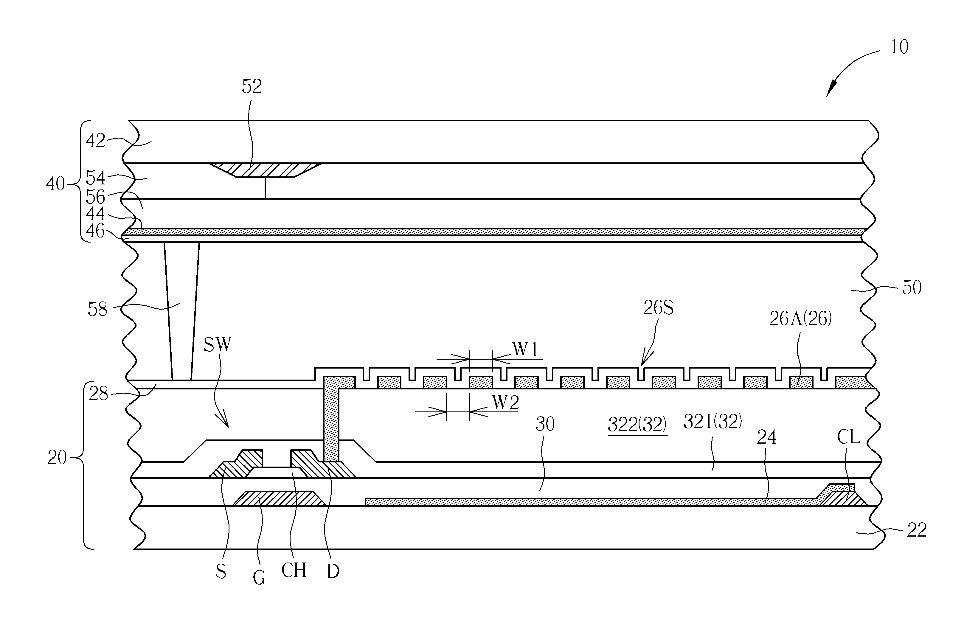
[0032]Refer to FIG. 1. FIG. 1 is a schematic diagram illustrating a display panel according to the present disclosure. The display panel of this embodiment includes a plurality of pixels, and each pixel includes a plurality of sub-pixels. To highlight the features of the display panel of the present disclosure, only one single sub-pixel is exemplarily drawn in FIG. 1. In addition, an FFS display panel is selected as an example of the display panel in this embodiment, but not limited. As shown in FIG. 1, the display panel 10 of this embodiment includes a first substrate structure 20, a second substrate structure 40 and a non-self-luminous display medium layer 50. The first substrate structure 20 includes a first substrate 22, a first common electrode 24, a pixel electrode 26 and a first alignment film 28. The first common electrode 24 is disposed on the first substrate 22. The pixel electrode 26 is disposed on the first common electrode 24, the pixel electrode 26 and the first common...

second embodiment

[0043]Refer to Table 1. Table 1 lists an optimal configuration of the dielectric constant and the thickness of the first passivation layer 321, the second passivation layer 322, the first alignment film 28, the non-self-luminous display medium layer 50 and the second alignment film 46 of the display panel 10′ in the

TABLE 1dielectricthicknessunit capacitanceconstant(Angstrom)(farad / μm2)first passivation5.420002.391*10−16layersecond3.2300009.444*10−18passivation layerfirst alignment38003.320*10−16filmnon-self-luminous3.5320009.6840*10−18 display mediumlayersecond alignment38003.320*10−16film

[0044]Refer to FIG. 5, as well as Table 1. FIG. 5 illustrates a relation between the second capacitance / the first capacitance and the thickness of the second passivation layer, where the ratio of the second capacitance to the first capacitance is unit free, and the unit of thickness of the second passivation layer is angstrom. As shown in FIG. 5, when the dielectric constant and the thickness of th...

fourth embodiment

[0057]Refer to FIG. 13. FIG. 13 is a schematic diagram illustrating a display panel according to the present disclosure. As shown in FIG. 13, in the display panel 80 of this embodiment, the branch electrodes 68A of the pixel electrode 68 are arranged along the second direction D2, instead of along the first direction D1. The branch electrodes 68A and the data line DL may have at least one turning part. In this embodiment, the shape of the common line CL may be modified as disclosed in the alternative embodiments of FIGS. 10A-10E, and the relation between the width of the light-shielding layer 722 and the width of the transparent electrode layer 721 of the light-blocking stacking layer 72 may be modified as disclosed in the embodiments of FIGS. 9, 11 and 12. Furthermore, transparent electrode layer 721 does not exist on (or namely is not disposed on) the effective light-transmitting region in FIGS. 9 to 13, for example.

[0058]Refer to FIG. 14 and FIG. 15. FIG. 14 is a simulation diagr...


PUM


Abstract

A display panel includes a first substrate structure, a second substrate structure and a non-self-luminous display medium layer. The first substrate structure includes a first substrate, a first common electrode, a pixel electrode and a first alignment film. The second substrate structure is disposed opposite to the first substrate structure. The second substrate structure includes a second substrate, a second common electrode and a second alignment film. The non-self-luminous display medium layer is interposed between the first alignment film and the second alignment film. A first capacitance is formed between the first common electrode and the pixel electrode, a second capacitance is formed between the pixel electrode and the second common electrode, and a ratio of the second capacitance to the first capacitance is substantially between 0.7 and 1.3.

Description

BACKGROUND OF THE DISCLOSURE[0001]1. Field of the Disclosure[0002]The present disclosure relates to a display panel, and more particularly, to a display panel having symmetrical capacitor design with low light leakage.[0003]2. Description of the Related Art[0004]Liquid crystal display (LCD) panel has been widely used in various types of display devices for its advantages such as compact size, good display quality and low power consumption. The conventional LCD panel (e.g. twisted nematic (TN) LCD panel) suffers from the narrow viewing angle problem, and thus the applications of conventional LCD are limited.[0005]In order to address the narrow viewing angle problem of TN LCD panel, several types of wide viewing angle LCD panels such as in-plane switching (IPS) LCD panels and fringe field switching (FFS) LCD panels have been proposed. The conventional IPS LCD panel and the FFS LCD panel have wide viewing angle, but they still suffer from some drawbacks such as low light transmittance,...

Claims


Application Information

Patent Timeline
Patent Type & Authority Applications(United States)
IPC IPC(8): H01L27/12
CPCH01L27/124H01L27/1255G02F1/133512G02F1/134363G02F1/136213G02F1/134372
Inventor LEE, SEOK-LYULCHEN, YI-CHINGCHANG, CHE-CHIATSENG, CHIN-ANKUO, YU-CHIEH
Owner AU OPTRONICS CORP
Why Eureka
Try Eureka