
Transient voltage suppressor and its manufacturing method

a technology of transient voltage and suppressor, which is applied in the direction of diodes, semiconductor devices, electrical apparatus, etc., can solve the problems of affecting the overall current flowing through and it is difficult to adopt the transient voltage suppressor tv to a high-frequency circuit, so as to achieve the effect of easy control of voltage and the characteristics of a zener diod

Active Publication Date: 2015-04-30
KEC
View PDF30 Cites 6 Cited by
  • Summary
  • Abstract
  • Description
  • Claims
  • Application Information

AI Technical Summary

Benefits of technology

This patent is about a method and device called a transient voltage suppressor, which can control the voltage a Zener diode can handle. The method involves creating two parts of a layer called a buried layer by using ion implantation and depositing layers of the same impurity concentration. This allows for easy control of the voltage withstanding characteristics of the Zener diode. Additionally, the method includes creating a specific doping region in a ring shape to increase the current pass region and improve the current distribution of the Zener diode in a small area. Overall, this patent provides a way to handle high voltages with a Zener diode and improve its performance in a compact space.

Problems solved by technology

The increase in the capacitance value of the transient voltage suppressor TVS may severely distort signals, making it difficult to adopt the transient voltage suppressor TVS to a high-frequency circuit.
In addition, since a breakdown voltage of the transient voltage suppressor TVS is considerably affected by a concentration difference between the substrate and the doping region, affecting the overall current flowing throughout the transient voltage suppressor TVS.

Method used


Image

  • Transient voltage suppressor and its manufacturing method
  • Transient voltage suppressor and its manufacturing method
  • Transient voltage suppressor and its manufacturing method

Examples


Embodiment Construction

[0035]The present invention now will be described more fully hereinafter with reference to the accompanying drawings, in which embodiments of the invention are shown. This invention may, however, be embodied in many different forms and should not be construed as limited to the embodiments set forth herein. Rather, these embodiments are provided so that this disclosure will be thorough and complete, and will fully convey the scope of the invention to those skilled in the art.

[0036]The terminology used herein is for the purpose of describing particular embodiments only and is not intended to be limiting of the invention. As used herein, the singular forms “a”, “an” and “the” are intended to include the plural forms as well, unless the context clearly indicates otherwise. It will be further understood that the terms “comprises” and / or “comprising,” when used in this specification, specify the presence of stated features, integers, steps, operations, elements, and / or components, but do ...


PUM


Abstract

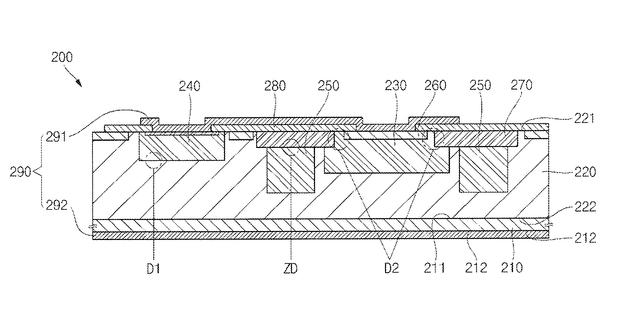
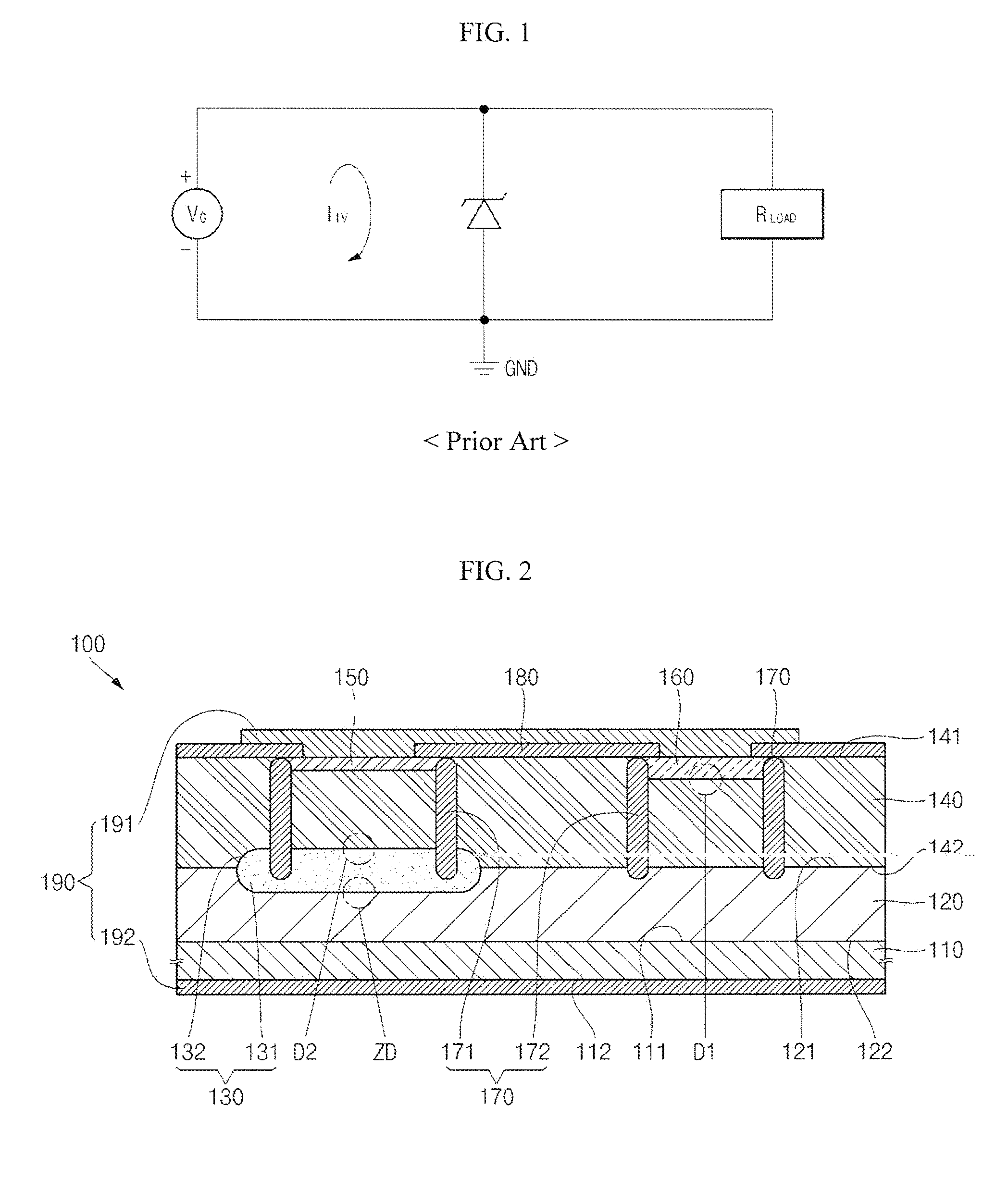
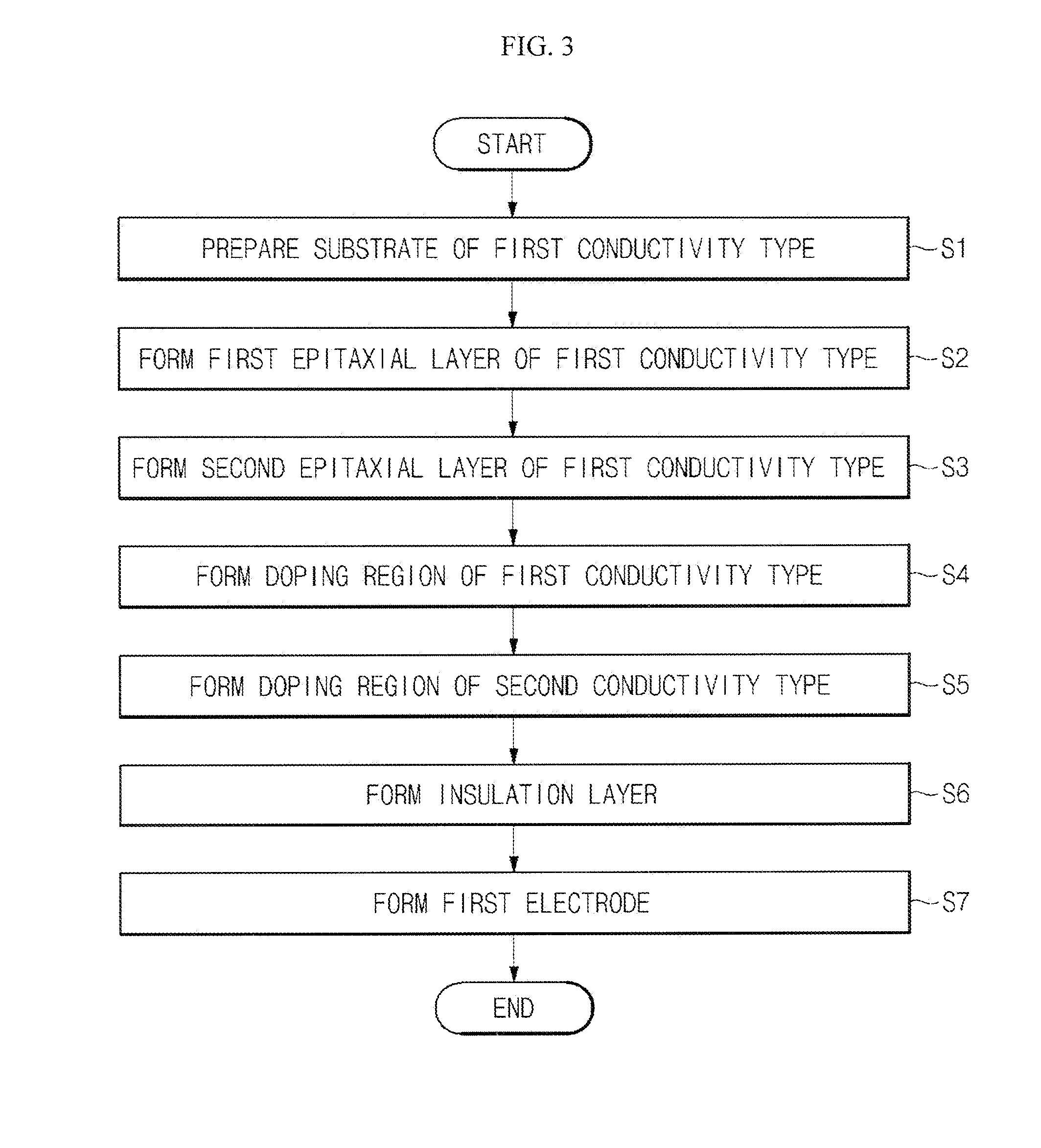
A transient voltage suppressor and its manufacturing method are provided, which can easily control voltage withstanding characteristics of a Zener diode by analogizing growth of a buried layer by forming a portion of the buried layer by performing ion implantation on a first epitaxial layer and then forming the other portion of the buried layer while depositing a second epitaxial layer having the same impurity concentration with the first epitaxial layer, and which can improve a current distribution characteristic by forming a doping region in a ring shape to increase a current pass region by increasing a PN junction area of a Zener diode in a small area.

Description

CROSS-REFERENCE TO RELATED APPLICATION[0001]This application claims priority to and the benefit of Korean Patent Application No. 10-2013-0131808 filed on Oct. 31, 2013, which is herein incorporated by reference in its entirety.BACKGROUND OF THE INVENTION[0002]1. Field of the Invention[0003]Aspects of the present invention relate to a transient voltage suppressor and its manufacturing method.[0004]2. Description of the Related Art[0005]Referring to FIG. 1, a circuit view for the operating principle of a general transient voltage suppressor is illustrated. As illustrated in FIG. 1, the general transient voltage suppressor (TVS) (e.g., a varistor, a thyristor, or a diode (rectifier / Zener)) is connected in parallel between a power supply VG and a load RLOAD, and one side of the transient voltage suppressor TVS is connected to a ground (GND).[0006]With this configuration, when an over-voltage exceeding a voltage required by the load RLOAD is input, a transient voltage derived current (IT...

Claims


Application Information

Patent Timeline
Patent Type & Authority Applications(United States)
IPC IPC(8): H01L27/02H01L29/66H01L21/265H01L29/861
CPCH01L27/0248H01L21/265H01L29/6609H01L29/861H01L27/0255H01L29/866
Inventor KIM, HYUN SIKJANG, HEE WON
Owner KEC
Learn More