Antenna device and electronic apparatus

a technology of electronic equipment and antenna device, applied in the direction of antenna, antenna details, elongated active element feed, etc., can solve the problems of inability to communicate, difficult to secure the space necessary for the antenna, and difficulty in forming and integrating antennas applied in a plurality of frequency bands, so as to achieve the effect of significantly reducing the size of the antenna devi

Active Publication Date: 2015-04-30
MURATA MFG CO LTD
View PDF3 Cites 58 Cited by
  • Summary
  • Abstract
  • Description
  • Claims
  • Application Information

AI Technical Summary

Benefits of technology

[0026]According to various preferred embodiments of the present invention, a radiation element is configured to define and function as a field emission element in a first frequency band and function as a magnetic field emission element in a second ...

Problems solved by technology

Housings, which used to be made of resin, of small communication terminal apparatuses, such as cellular phone terminals, have their entire surface plated with metal or the like in order to counter a degradation in the mechanical strength associated with the reduction in the size and thickness of the housings, and thus the housings are being “metalized.” However, if an antenna is embedded inside a metalized...

Method used


Image

  • Antenna device and electronic apparatus
  • Antenna device and electronic apparatus
  • Antenna device and electronic apparatus

Examples


first preferred embodiment

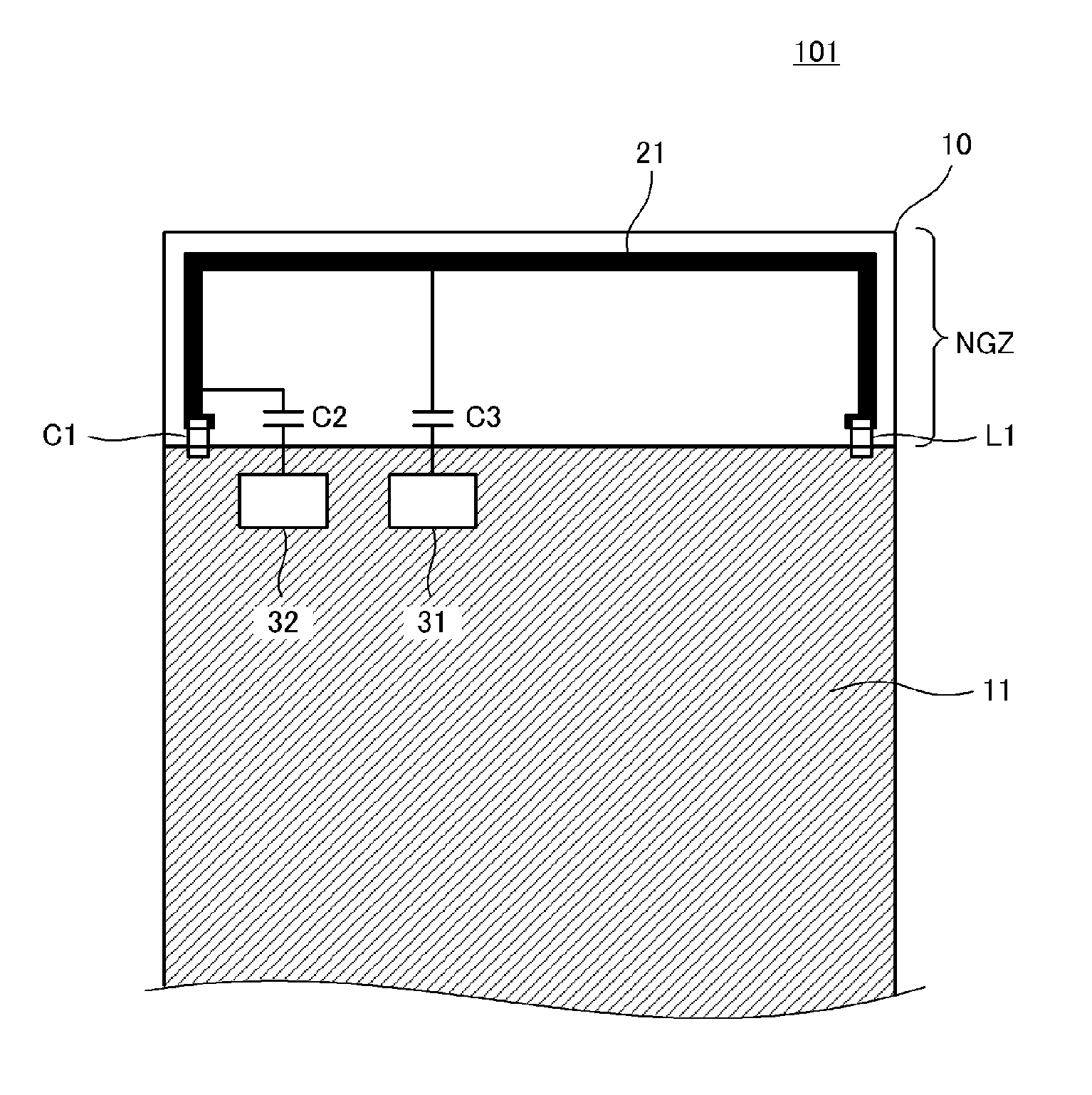
[0048]FIG. 1 is a plan view of a primary portion of an antenna device 101 according to a first preferred embodiment of the present invention. This antenna device 101 is provided on a board 10. The board 10 includes a region where a ground conductor 11 is located and a non-ground region NGZ where the ground conductor is not located. A square bracket-shaped radiation element 21 is located in the non-ground region NGZ. Specifically, this radiation element 21 includes a portion that is parallel or substantially parallel to an edge side of the ground conductor 11 and portions that extend from the parallel portion toward the ground conductor. A chip capacitor (capacitor) C1 is mounted between a first end of the radiation element 21 and the ground conductor 11 and is electrically connected therebetween. In addition, a chip inductor L1 is mounted between a second end of the radiation element 21 and the ground conductor 11 and is electrically connected therebetween. The inductor L1 correspon...

second preferred embodiment

[0061]In a second preferred embodiment of the present invention, an example in which the second feeder circuit carries out a balanced feed to an antenna will be illustrated.

[0062]FIG. 5 is a plan view of a primary portion of an antenna device 102 according to the second preferred embodiment. This antenna device 102 is provided on the board 10. The board 10 includes a region where the ground conductor 11 is located and the non-ground region NGZ where the ground conductor is not located. The square bracket-shaped radiation element 21 is located in the non-ground region NGZ. A circuit that includes a plurality of chip components and the second feeder circuit 32 is provided between the first end of the radiation element 21 and the ground conductor 11. The chip inductor L1 is connected between the second end of the radiation element 21 and the ground conductor 11. Other configurations are preferably similar to those illustrated in FIG. 1.

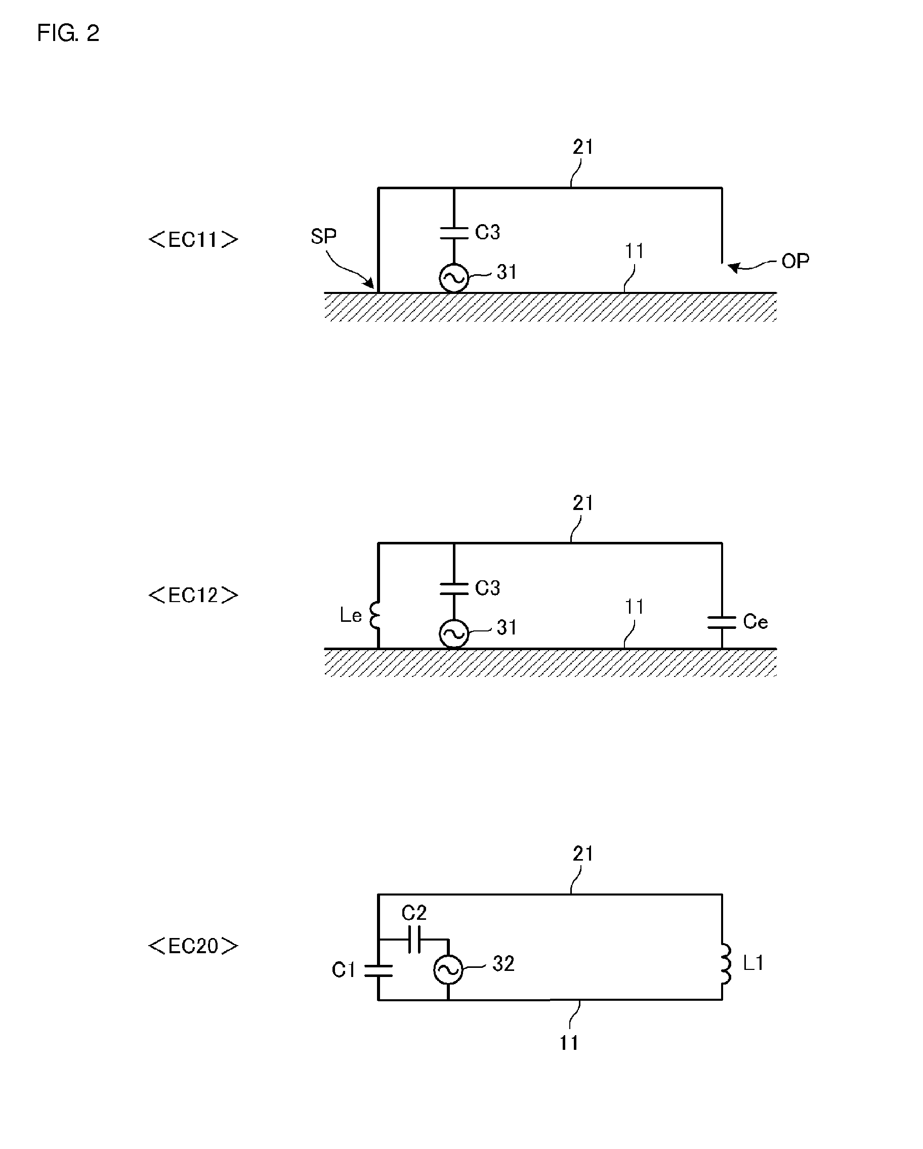
[0063]FIG. 6 illustrates an equivalent circuit dia...

third preferred embodiment

[0065]FIG. 7 is a plan view of a primary portion of an antenna device 103 according to a third preferred embodiment of the present invention. This antenna device 103 is provided on the board 10. The board 10 includes a region where the ground conductor 11 is located and the non-ground region NGZ where the ground conductor is not located. The square bracket-shaped radiation element 21 is located in the non-ground region NGZ. The first end of the radiation element 21 is directly grounded to the ground conductor 11. The chip inductor L1 and the chip capacitor C1 are connected in series between the second end of the radiation element 21 and the ground conductor 11.

[0066]On the board 10, the first feeder circuit 31 is defined by the UHF band IC, and the second feeder circuit 32 is defined by the HF band RFID IC.

[0067]The input / output portion of the first feeder circuit is connected to a predetermined feeding point of the radiation element 21 through the capacitor C3. Meanwhile, the input...


PUM


Abstract

A square bracket-shaped radiation element is in a non-ground region of a board. A first reactance element that equivalently enters a short-circuited state in a second frequency band is connected between a second end of the radiation element and a ground conductor. A second reactance element that equivalently enters a short-circuited state in a first frequency band s connected between a first end of the radiation element and the ground conductor. In the UHF band, the radiation element and the ground conductor function as an inverted F antenna that contributes to field emission. In the HF band, a loop including the radiation element and the ground conductor functions as a loop antenna that contributes to magnetic field emission.

Description

BACKGROUND OF THE INVENTION[0001]1. Field of the Invention[0002]The present invention relates to antenna devices that are shared by communication systems that use communication signals in mutually different frequency bands and to electronic apparatuses that include such antenna devices.[0003]2. Description of the Related Art[0004]With recent advancements in functionality, antennas not only for voice communication but also for various communication (broadcasting) systems, such as a GPS, a wireless LAN, and terrestrial digital broadcasting, are being embedded in such systems.[0005]Japanese Unexamined Patent Application Publication No. 2007-194995, for example, discloses an antenna device that is shared by communication systems that use communication signals in mutually different frequency bands.[0006]Housings, which used to be made of resin, of small communication terminal apparatuses, such as cellular phone terminals, have their entire surface plated with metal or the like in order t...

Claims


Application Information

Patent Timeline
IPC IPC(8): H01Q5/328H01Q7/00H01Q5/10
CPCH01Q7/00H01Q5/328H01Q5/335H01Q5/371H01Q1/2216H01Q1/243H01Q9/42H01Q1/2208H01Q21/28
Inventor YOSUI, KUNIAKI
Owner MURATA MFG CO LTD
Why Eureka
Try Eureka