
Microwave induced plasma decapsulation using a dielectric plasma discharge tube

a dielectric plasma and plasma discharge technology, applied in the direction of electric discharge tubes, basic electric elements, electrical equipment, etc., can solve the problems of inapplicability of plasma etching system, inability to use rie plasma etch system for decapsulation, and limitations of wet-etch decapsulation process

Active Publication Date: 2015-04-30
NISENE TECH GROUP
View PDF12 Cites 3 Cited by
  • Summary
  • Abstract
  • Description
  • Claims
  • Application Information

AI Technical Summary

Benefits of technology

The patent text describes a method for safely and effectively decapsulating electronic devices that are encapsulated in plastic packaging or other resinous materials. The method uses a plasma etch process to remove the epoxy molding compound without causing damage to the chip or package elements. The technical effect of this method is that it allows for inspection, test, and repair of the chip or package elements without having to use concentrated acids or solvents for the resin, which can cause damage to the bond wires and other components. The method also avoids the need for high-temperature processing during the decapsulation process, which can cause damage to the semiconductor die.

Problems solved by technology

The wet-etch decapsulation process has its limitations when semiconductor devices employ Cu and Ag based bond wires.
Copper and silver alloy bond wires tend to suffer from etch damage when subjected to the conventional web-etch based decapsulation process.
However, using RIE plasma etch system for decapsulation is not practical as the decapsulation process could take several hours.
During such a decapsulation process, the semiconductor device is subjected to high temperature which may have the undesired consequence of healing bake recoverable failures on the semiconductor die.

Method used


Image

  • Microwave induced plasma decapsulation using a dielectric plasma discharge tube
  • Microwave induced plasma decapsulation using a dielectric plasma discharge tube
  • Microwave induced plasma decapsulation using a dielectric plasma discharge tube

Examples


Embodiment Construction

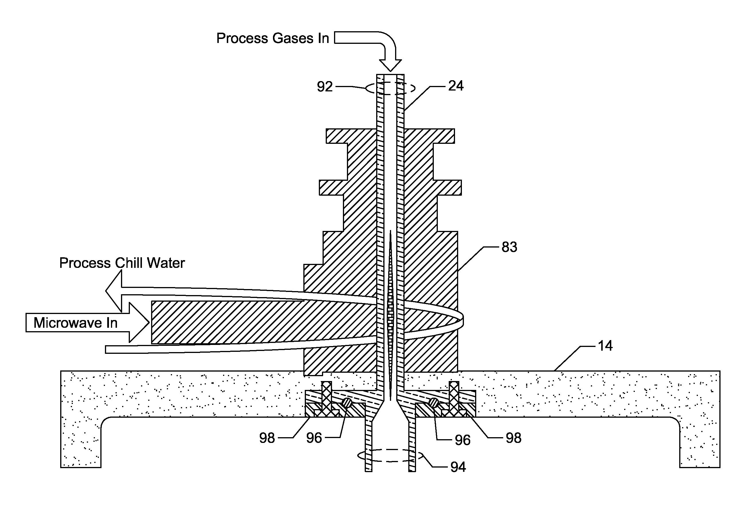
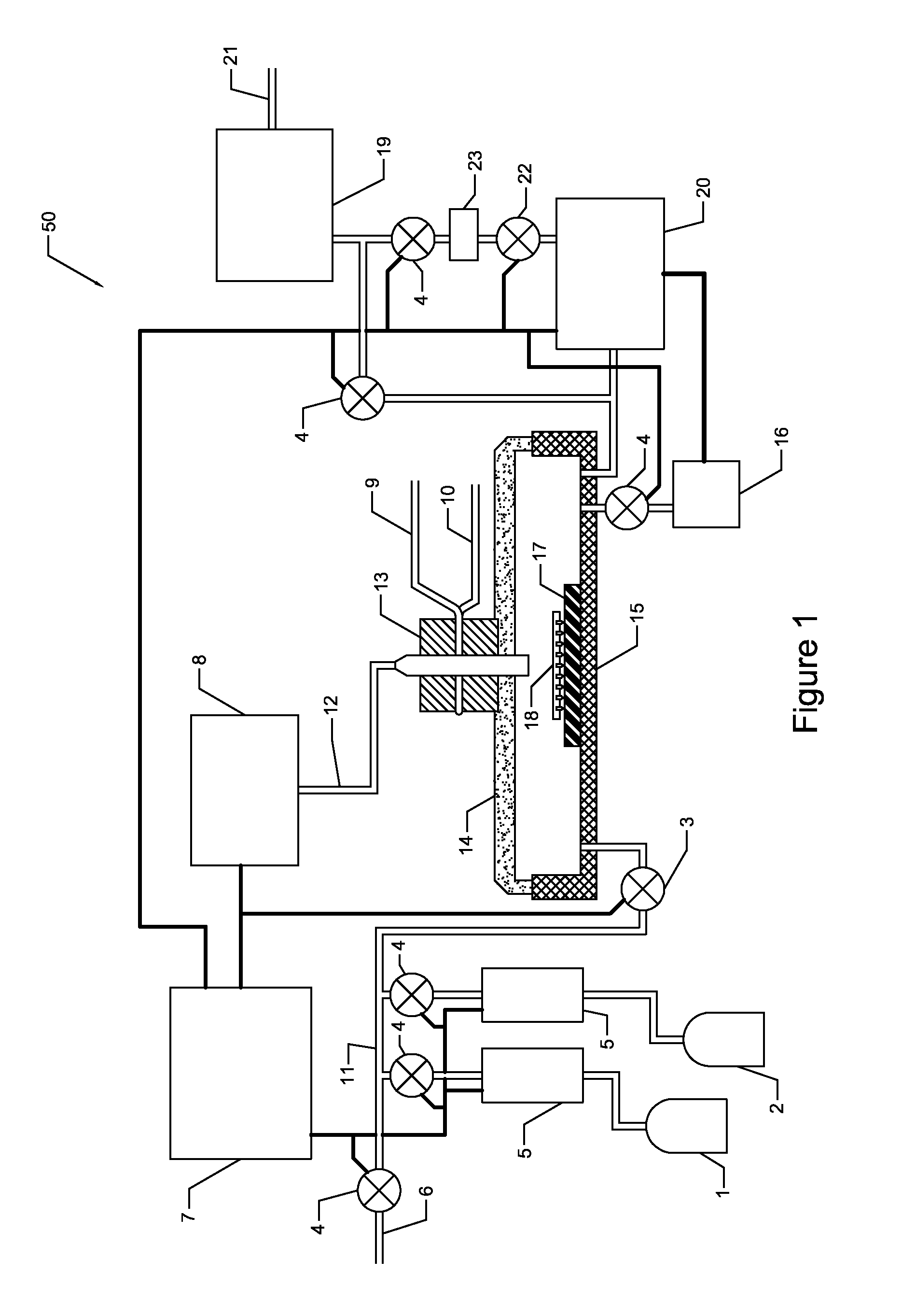
[0017]The invention can be implemented in numerous ways, including as a process; an apparatus; a system; and / or a composition of matter. In this specification, these implementations, or any other form that the invention may take, may be referred to as techniques. In general, the order of the steps of disclosed processes may be altered within the scope of the invention.

[0018]A detailed description of one or more embodiments of the invention is provided below along with accompanying figures that illustrate the principles of the invention. The invention is described in connection with such embodiments, but the invention is not limited to any embodiment. The scope of the invention is limited only by the claims and the invention encompasses numerous alternatives, modifications and equivalents. Numerous specific details are set forth in the following description in order to provide a thorough understanding of the invention. These details are provided for the purpose of example and the inv...


PUM

PropertyMeasurementUnit
Fractionaaaaaaaaaa
Pressureaaaaaaaaaa
Poweraaaaaaaaaa

Abstract

A microwave induced plasma decapsulation system and method for decapsulation a packaged semiconductor device applies a microwave induced plasma effluent along with etchant gases electrons, ions and free radicals that are chemically reactive to remove the epoxy molding compound encapsulating the semiconductor device. In one embodiment, the decapsulation system utilizes a microwave generator and a coaxial plasma source. In another embodiment, the decapsulation system utilizes a microwave generator, an electromagnetic surface wave plasma source, and a dielectric plasma discharge tube.

Description

CROSS REFERENCE TO OTHER APPLICATIONS[0001]This application claims priority to U.S. Provisional Patent Application No. 61 / 897,800, entitled MICROWAVE INDUCED PLASMA DECAPSULATION, filed Oct. 30, 2013, which is incorporated herein by reference for all purposes.BACKGROUND OF THE INVENTION[0002]Electronic devices with integrated circuit chips or semiconductor dies encapsulated in plastic packaging have been employed for some years. In the present description, an electronic device refers to a packaged semiconductor device incorporating one or more integrated circuit chips. Typically, an epoxy resin is molded around the semiconductor chip, a central portion of a lead frame and bonding wires or other connections between contact pads on the chip to inner lead fingers on the lead frame. It is sometimes necessary to decapsulate such a plastic-encapsulated package at least in part to allow for inspection, test and repair of the chip or the wire bonds to the chip, or the inner lead fingers, af...

Claims


Application Information

Patent Timeline
IPC IPC(8): H01L21/67H01L21/311
CPCH01L21/67126H01L21/67069H01L21/31138H01J37/32192H01L21/56
Inventor WAGNER, ALAN M.KRISHNAN, RAVIN
Owner NISENE TECH GROUP
Features
  • Generate Ideas
  • Intellectual Property
  • Life Sciences
  • Materials
  • Tech Scout
  • Unparalleled Data Quality
  • Higher Quality Content
  • 60% Fewer Hallucinations
Learn More