
Semiconductor circuit device, electronic device, electronic apparatus, and moving object

a technology of semiconductor circuit devices and electronic devices, applied in semiconductor devices, semiconductor/solid-state device details, oscillator generators, etc., can solve the problems of difficult to secure one large rectangular area, complicated connection and addressing of memory circuits, and memory malfunction, etc., to achieve high operational reliability, large area, and great flexibility in circuit arrangement

Active Publication Date: 2015-05-07
SEIKO EPSON CORP
View PDF5 Cites 5 Cited by
  • Summary
  • Abstract
  • Description
  • Claims
  • Application Information

AI Technical Summary

Benefits of technology

The patent text describes a semiconductor circuit device that can increase the storage capacity of its memory circuit without requiring a larger semiconductor substrate. The memory circuit is arranged in one rectangular area, making wiring and addressing easier than in multiple areas. This allows for a more flexible and reliable electronic apparatus that can be miniaturized. Additionally, the semiconductor circuit device also reduces interference between its circuit blocks and connection wires, resulting in higher operational reliability.

Problems solved by technology

In JP-A-2006-54269, the interference between the DC circuit block and the AC circuit block in the analog circuit block can be reduced, but there is a risk of causing a malfunction of a memory or the like as a digital circuit due to interference between the analog circuit and the digital circuit.
Moreover, since an arrangement of the connection pads is not considered, it may be difficult to secure one large rectangular area.
When the memory circuit is arranged in a plurality of areas, the connection and addressing of the memory circuit become complicated.

Method used


Image

  • Semiconductor circuit device, electronic device, electronic apparatus, and moving object
  • Semiconductor circuit device, electronic device, electronic apparatus, and moving object
  • Semiconductor circuit device, electronic device, electronic apparatus, and moving object

Examples


first embodiment

1-1. First Embodiment

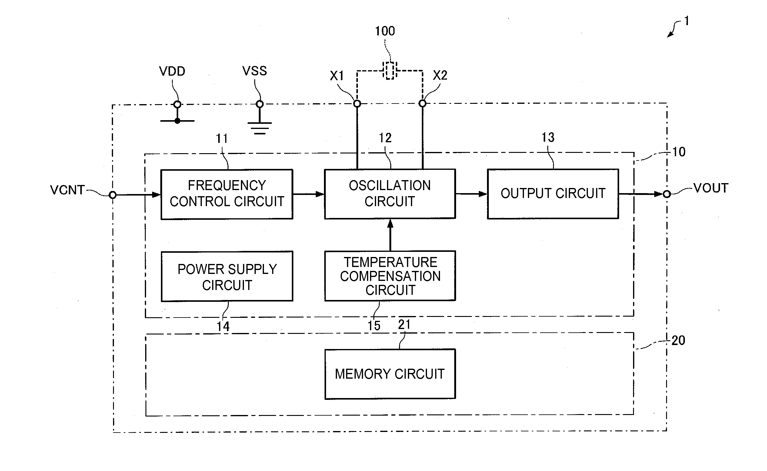
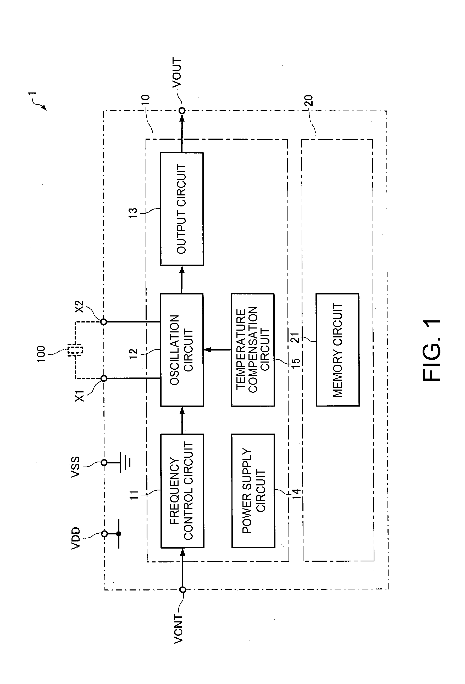
[0059]FIG. 1 is a circuit diagram showing an example of a semiconductor circuit device 1 according to this embodiment.

[0060]The semiconductor circuit device 1 according to the embodiment is configured to include a first circuit block 10 including an analog circuit as a component, a second circuit block 20 including a digital circuit as a component, a connection pad VDD, a connection pad VSS, a connection pad VCNT, a connection pad VOUT, a connection pad X1, and a connection pad X2.

[0061]In the embodiment, the first circuit block 10 is composed mainly of analog circuits, but may include a portion of one or more digital circuits. In the example shown in FIG. 1, the first circuit block 10 is configured to include a frequency control circuit 11, an oscillation circuit 12, an output circuit 13, a power supply circuit 14, and a temperature compensation circuit 15.

[0062]In the embodiment, the second circuit block 20 is composed mainly of digital circuits, but may inclu...

second embodiment

1-2. Second Embodiment

[0097]FIG. 3 is a plan view schematically showing the layout of a semiconductor circuit device 1a according to this embodiment. The circuit configuration of the semiconductor circuit device 1a is the same as the circuit configuration shown in FIG. 1. In FIG. 3, portions of circuits included in the first circuit block 10 and the second circuit block 20 are not illustrated.

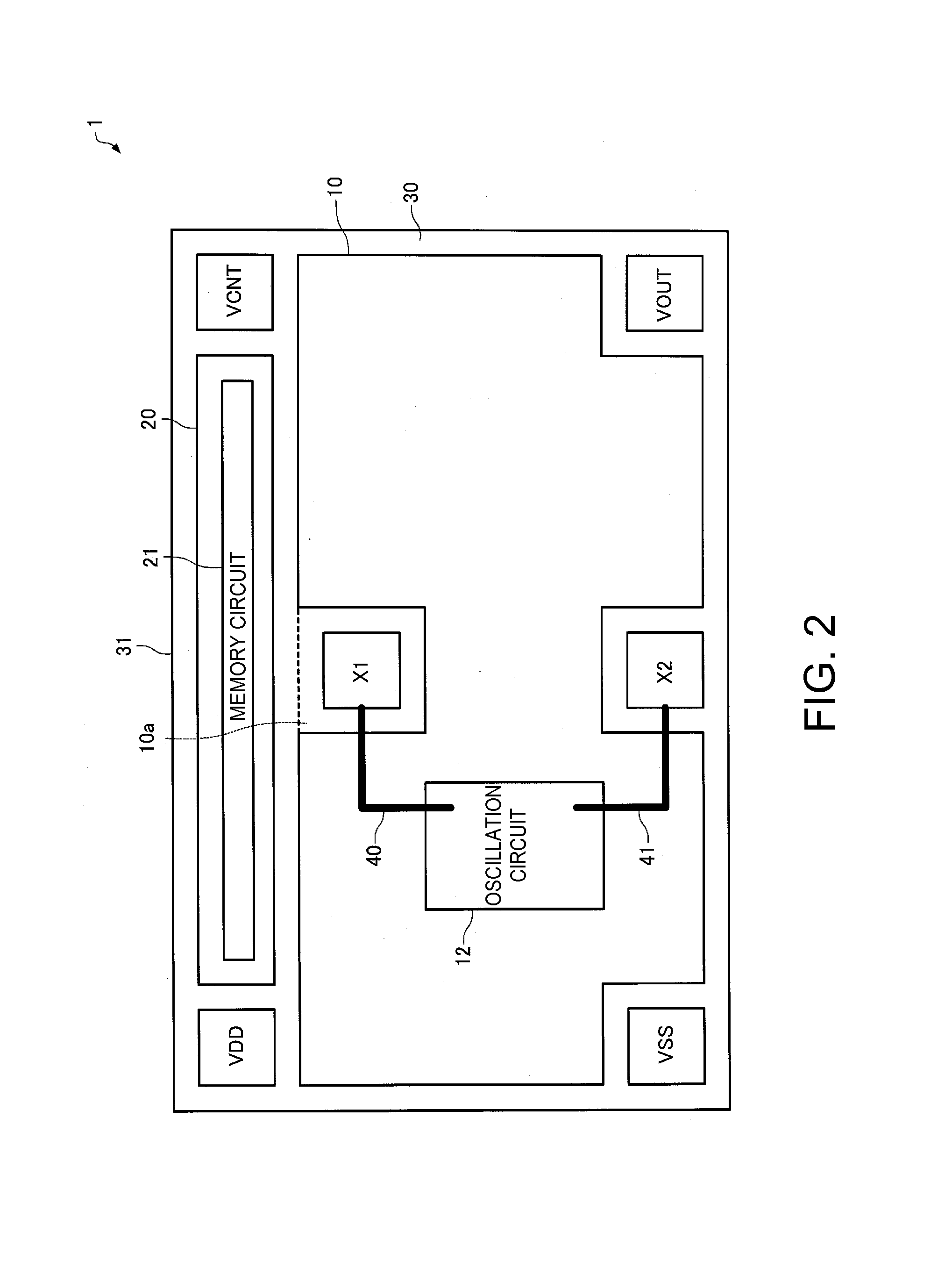
[0098]In the example shown in FIG. 2, the connection pad VDD, the second circuit block 20, and the connection pad VCNT are provided in this order so as to be along the long side (the edge portion 31) of the semiconductor substrate 30. In the example shown in FIG. 3, however, the connection pad VDD, the second circuit block 20, the first circuit block 10, and the connection pad VCNT are provided in this order so as to be along the long side (the edge portion 31) of the semiconductor substrate 30. That is, in the example shown in FIG. 3, a portion of the first circuit block 10 is provided to jut ...

third embodiment

1-3. Third Embodiment

[0100]FIG. 4 is a plan view schematically showing the layout of a semiconductor circuit device 1b according to this embodiment. The circuit configuration of the semiconductor circuit device 1b is the same as the circuit configuration shown in FIG. 1. In FIG. 4, portions of circuits included in the first circuit block 10 and the second circuit block 20 are not illustrated.

[0101]In the embodiment, the connection pad VCNT (an example of a second connection pad) is included, and the second circuit block 20 is provided between the edge portion 31 and the first circuit block 10 and between the edge portion 31 and the connection pad VCNT (an example of the second connection pad) in the plan view. Moreover, the second circuit block 20 is provided between the edge portion 31 and the connection pad X1 in the plan view.

[0102]According to the embodiment, one rectangular area much larger than that of the first embodiment can be secured in the second circuit block 20 arranged...


PUM


Abstract

A semiconductor circuit device includes: a semiconductor substrate; and a first circuit block including an analog circuit as a component, a second circuit block including a digital circuit as a component, a connection pad, and a connection wire electrically connecting the connection pad with the first circuit block, all of which are arranged on the semiconductor substrate. The connection wire is provided so as not to overlap the second circuit block in a plan view.

Description

BACKGROUND[0001]1. Technical Field[0002]The present invention relates to a semiconductor circuit device, an electronic device, an electronic apparatus, and a moving object.[0003]2. Related Art[0004]Oscillators using a vibrator such as a quartz crystal resonator (piezoelectric vibrator) or a MEMS (Micro Electro Mechanical Systems) vibrator are known. In many of these oscillators, a configuration including a memory circuit that stores various kinds of setting information is adopted in addition to an oscillation circuit.[0005]JP-A-2006-54269 discloses a configuration for improving a characteristic degradation such as phase noise due to interference between a DC (direct current) circuit block and an AC (alternating current) circuit block located in an analog circuit block. To accomplish this, the DC circuit block and the AC circuit block in the analog circuit block are arranged separate from each other and a digital circuit block, such as for a memory, is arranged therebetween.[0006]JP-...

Claims


Application Information

Patent Timeline
IPC IPC(8): H01L23/552H03B5/32
CPCH03B5/32H01L23/552H01L23/528H01L24/06H01L24/16H03H9/1071H01L2224/0401H01L2224/06135H01L2224/06164H01L2224/16225H01L2924/1434H01L2924/1461H01L2924/15153H01L2924/1517H01L2924/15313H01L2924/15323H01L2924/16195H03H9/02102H03H9/0552
Inventor ITASAKA, YOSUKEISHIKAWA, MASAYUKIYAMAMOTO, TAKEHIRO
Owner SEIKO EPSON CORP
Learn More