Method for manufacturing semiconductor device and annealing method

a manufacturing method and technology of semiconductor devices, applied in semiconductor/solid-state device manufacturing, basic electric elements, electric devices, etc., can solve the problems of insufficient removal of impurity doping-generated defects, leakage current in the operation of the device, and most of crystal defects to be left behind. , to achieve the effect of sufficient removal of crystal defects

Inactive Publication Date: 2015-05-14
TOKYO ELECTRON LTD
View PDF3 Cites 9 Cited by
  • Summary
  • Abstract
  • Description
  • Claims
  • Application Information

AI Technical Summary

Benefits of technology

[0006]In view of the above, the present invention provides a manufacturing method of a semiconductor device and an annealing method capable of sufficiently removing crystal defects even at a low temperature in impurity activation annealing after doping impurities into a semiconductor substrate.

Problems solved by technology

However, in the annealing technique at a low temperature, defects generated during impurity doping may not be removed sufficiently.
Particularly, when performing the SPE after performing the impurity doping in the amorphized region, most of crystal defects may remain in an end portion of the initially amorphized region.
The remaining defects cause leakage current in the operation of the device.

Method used


Image

  • Method for manufacturing semiconductor device and annealing method
  • Method for manufacturing semiconductor device and annealing method
  • Method for manufacturing semiconductor device and annealing method

Examples


Embodiment Construction

[0018]Hereinafter, an embodiment of the present invention will be described in detail with reference to the accompanying drawings.

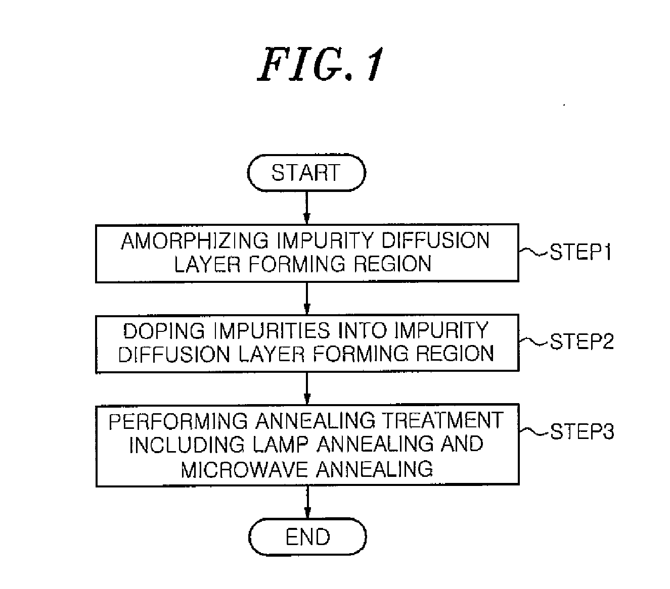
[0019]FIG. 1 is a flowchart showing a manufacturing method of a semiconductor device in accordance with an embodiment of the present invention.

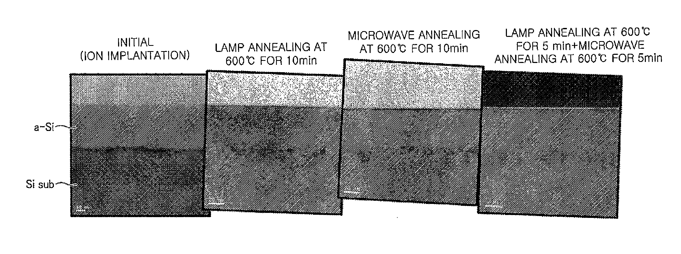
[0020]First, an impurity diffusion layer forming region of a semiconductor wafer (semiconductor substrate) is amorphized at step 1. As examples of an impurity diffusion layer, there are a source electrode and a drain electrode of a MOS type semiconductor device.

[0021]By amorphizing the impurity diffusion layer forming region in this way, it is possible to increase the controllability of an implantation depth. Further, since a crystal grain boundary does not exist, impurity doping in the next step can be easily performed. Thus, even if subsequent annealing treatment is performed at a low temperature, activation of impurities and recrystallization (SPE) are possible.

[0022]In order to amorphize the impurity diffusion ...


PUM

PropertyMeasurementUnit
temperatureaaaaaaaaaa
frequencyaaaaaaaaaa

Abstract

A semiconductor device manufacturing method includes: amorphizing the impurity diffusion layer formation region; doping the impurity diffusion layer formation region of the semiconductor substrate with impurities; and performing an annealing treatment including lamp annealing in which a heating lamp is used and microwave annealing in which microwaves are irradiated, on the semiconductor substrate doped with the impurities, for activating the impurities. In addition to activation of the impurity, re-crystallization and removing of crystal defects also take place in the annealing treatment.

Description

FIELD OF THE INVENTION[0001]The present invention relates to a manufacturing method of a semiconductor device and an annealing method for forming an impurity diffusion layer by performing activation annealing after doping a semiconductor substrate with impurities.BACKGROUND OF THE INVENTION[0002]In a manufacturing process of a semiconductor device, there is a process of forming an impurity diffusion layer by performing impurity activation annealing after introducing impurities into a semiconductor substrate. Conventionally, lamp annealing of a short-time heat treatment at a high temperature of 1000° C. or more is performed as an activation treatment of impurities.[0003]Recently, with the miniaturization of the design rule of the semiconductor device, an annealing technique is demanded to suppress the thermal diffusion of impurities, and an annealing technique at a lower temperature has been studied. Further, as a technique for preventing diffusion of impurities, a technique using SP...

Claims


Application Information

Patent Timeline
Patent Type & Authority Applications(United States)
IPC IPC(8): H01L21/324H01L21/22
CPCH01L21/22H01L21/324H01L21/26506H01L21/26513H01L21/67115H01L21/67248H01L21/68742
Inventor WATANABE, YOSHIMASASHIRAGA, KENTARO
Owner TOKYO ELECTRON LTD
Why Eureka
Try Eureka