Comparator circuit, imaging apparatus using the same, and method of controlling comparator circuit

a comparator circuit and imaging apparatus technology, applied in the field of comparator circuits and imaging apparatuses using the same, can solve the problems of limited insufficient input voltage range of the comparator with respect to the input voltage range of the pixel signal

Active Publication Date: 2015-05-21
CANON KK
View PDF1 Cites 18 Cited by
  • Summary
  • Abstract
  • Description
  • Claims
  • Application Information

AI Technical Summary

Problems solved by technology

However, in an offset voltage canceling method described in Japanese Patent Application Laid-Open No. 2010-16656, an input voltage range of the comparator is limited depending on a voltage between a gate and a source of a transistor which constitutes a current mirror circuit of a comparator.
For this reason, depending on the performance of the transistor, the input voltage range of the comparator may not be sufficiently wide with respect to the input voltage range of the pixel signal.

Method used


Image

  • Comparator circuit, imaging apparatus using the same, and method of controlling comparator circuit
  • Comparator circuit, imaging apparatus using the same, and method of controlling comparator circuit
  • Comparator circuit, imaging apparatus using the same, and method of controlling comparator circuit

Examples


first embodiment

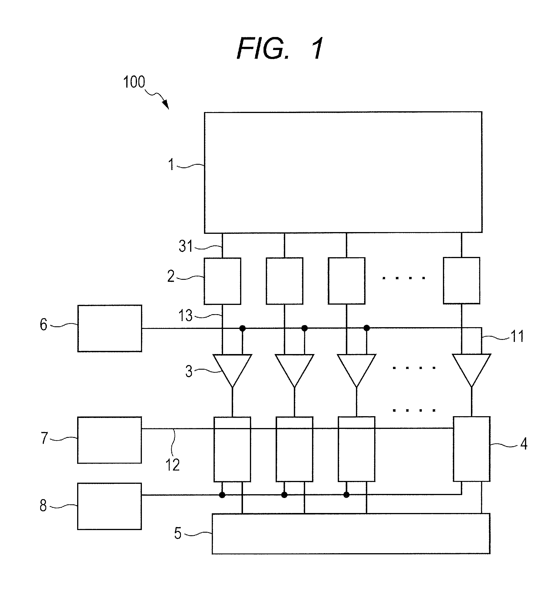
[0022]An imaging apparatus according to a first embodiment of the present invention and a comparator which is included in an A / D converter provided in each column of the imaging apparatus will be described below. FIG. 1 is a schematic view illustrating a circuit configuration of an imaging apparatus according to the first embodiment of the present invention. An imaging apparatus 100 includes: a pixel unit 1, a plurality of readout circuits 2, a plurality of comparing units 3, a plurality of storage units 4, a horizontal scanning circuit 5, a reference signal generating unit 6, a counter circuit 7, and a signal processing circuit 8.

[0023]The pixel unit 1 includes a plurality of pixels arranged in rows and columns. Each of the pixels outputs signals to a plurality of output lines 31 of the pixel signal, which is arranged for every pixel line, respectively.

[0024]Each of the readout circuits 2 is connected to each of the pixel columns in the pixel unit 1 through each of the output lines...

second embodiment

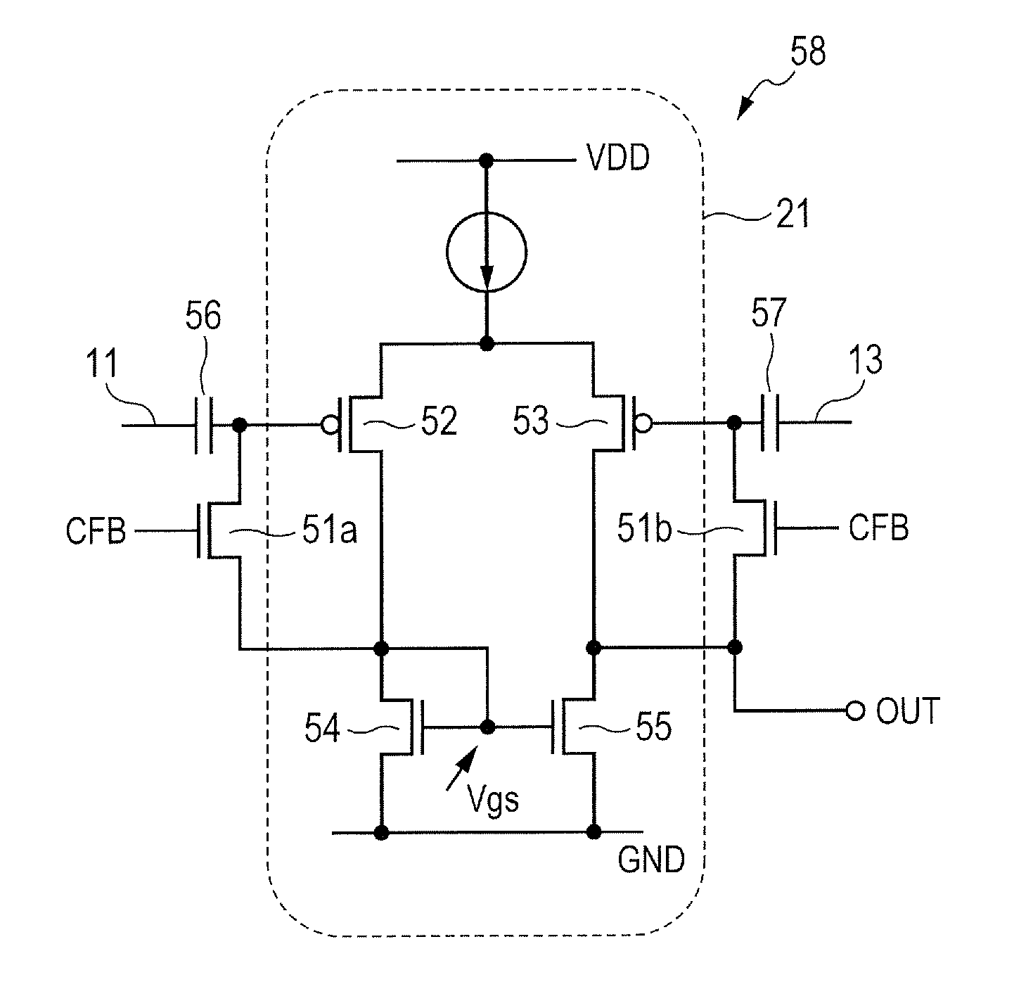
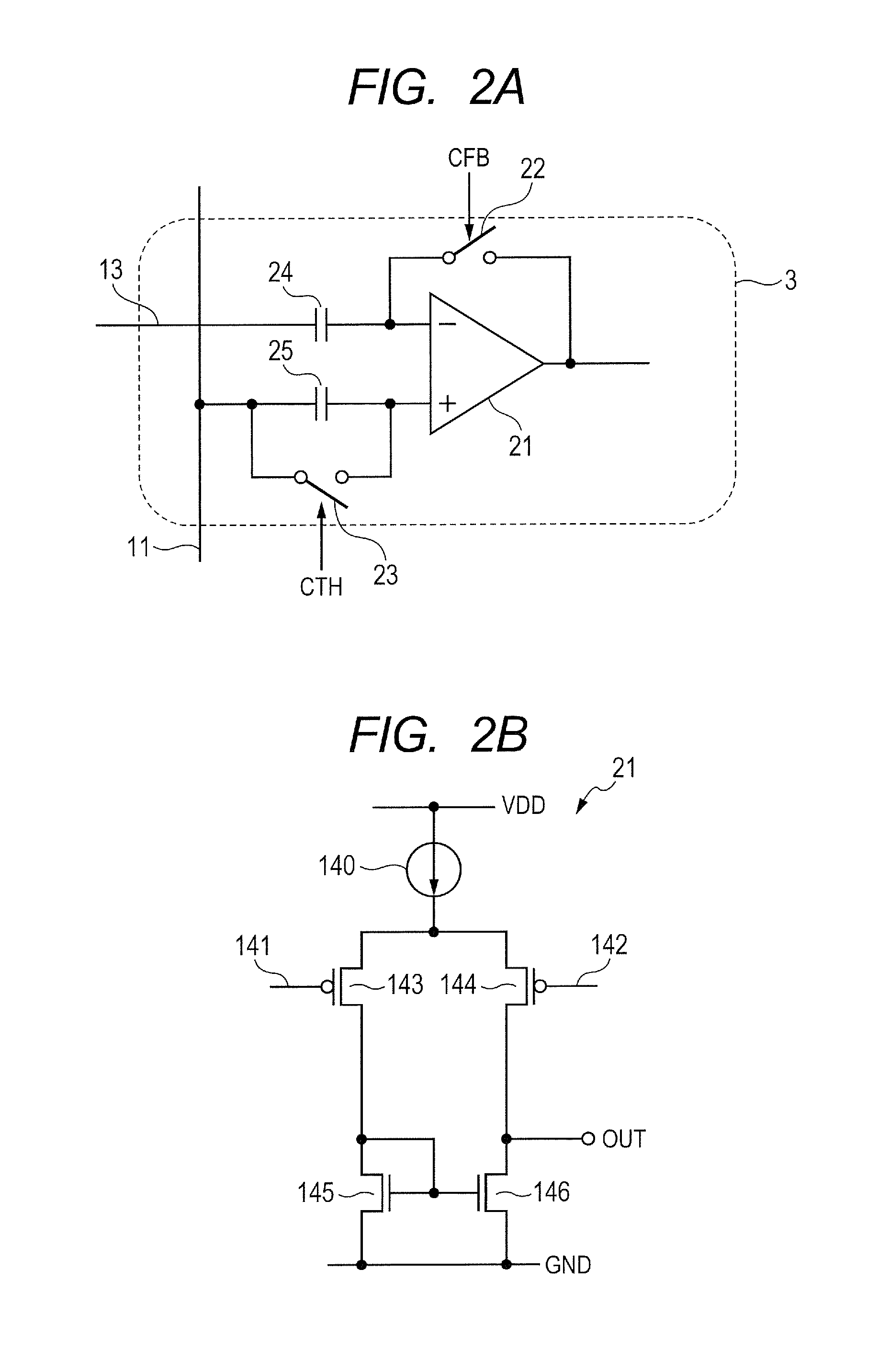
[0069]A comparator according to a second embodiment of the present invention will be described below. Incidentally, elements and wirings having similar functions as those in the first embodiment are designated by the same reference numerals, and the description will be occasionally omitted. FIG. 10 illustrates a circuit configuration of a comparing unit 73 which uses a comparator 21 according to the second embodiment of the present invention. The comparing unit 73 includes the comparator 21, an FB switch 22, a first input capacitor 24, a second input capacitor 25 and a potential supply switch 71. A fixed potential supply line 72 is connected to a non-inverting input terminal of the comparator 21 through the potential supply switch 71. Furthermore, to the non-inverting input terminal of the comparator 21, one end of the second input capacitor 25 is connected in parallel with the fixed potential supply line 72. The RAMP wiring 11 is connected to the other end of the second input capac...

third embodiment

[0075]A third embodiment of the present invention will be described below. FIG. 12 is a view illustrating a circuit configuration of a pixel 1a and a circuit configuration of a readout circuit 132 according to the third embodiment of the present invention. A point in which the third embodiment is different from the first and second embodiments is that the column amplifier of the readout circuit is omitted. Therefore, the previous output line 31 of the pixel signal is connected to the output line 13 of the readout circuit, and the potential of the output line 13 of the readout circuit is output intact as the potential of the output line 31 of the pixel signal. In the subsequent description, both of the wirings shall be integrally referred to as the output line 13 of the readout circuit. The other descriptions are similar to the above description, and accordingly the description will be omitted.

[0076]An operation of the comparing unit 3 according to the present embodiment will be desc...


PUM


Abstract

An object of the present invention is to provide a comparator which has an input voltage range larger than the case where a conventional offset cancel technique is used, while reducing an offset voltage. A comparator circuit includes: a comparator having an inverting input terminal, a non-inverting input terminal and an output terminal; a first switch having one terminal connected to the inverting input terminal and having the other terminal connected to the output terminal; a first capacitor which has one end connected with the inverting input terminal; a first signal input terminal which is another end of the first capacitor; and a second signal input terminal which selectively inputs either one of a fixed voltage and a comparing signal into the non-inverting input terminal.

Description

BACKGROUND OF THE INVENTION1. Field of the Invention[0001]The present invention relates to a comparator circuit, an imaging apparatus using the same, and a method of controlling the comparator circuit.[0002]2. Description of the Related Art[0003]Generally, a configuration of an analog-digital (A / D) converter includes a comparator. The A / D converter is used, for instance, for an imaging apparatus. For the imaging apparatus, there is a technique of connecting the A / D converter to each column of pixels arranged in rows and columns, and converting an analog signal output from each of the pixels into digital data by the A / D converter. Some A / D converters include a differential-input and single-end-output type comparator. There is a variation of offset voltage between input terminals of each of the comparators, among each of the columns. As a method of reducing this variation, a technique is known which cancels an offset voltage as described in Japanese Patent Application Laid-Open No. 20...

Claims


Application Information

Patent Timeline
Patent Type & Authority Applications(United States)
IPC IPC(8): H04N5/378H04N5/3745H03K5/125
CPCH04N5/378H04N5/37455H03K5/125H03K5/249H03M1/1295H03M1/56H04N25/77H04N25/75H04N25/772
Inventor NAKAMURA, KOHICHIKOBAYASHI, HIDEOHIYAMA, HIROKIYAMAZAKI
Owner CANON KK
Why Eureka
Try Eureka