
Liquid crystal display device

a liquid crystal display and display screen technology, applied in non-linear optics, instruments, optics, etc., can solve the problems of difficult to form a height difference around the through-hole, occurrence of sesame-like pixel defects, and difficulty in using organic passivation films, etc., to achieve the effect of reducing the area

Active Publication Date: 2015-05-21
JAPAN DISPLAY INC
View PDF3 Cites 12 Cited by
  • Summary
  • Abstract
  • Description
  • Claims
  • Application Information

AI Technical Summary

Benefits of technology

The patent is about a liquid crystal display device that can prevent display irregularities caused by thickness irregularities of the orientation film. This is achieved by designing a high definition screen with small pixels and through-holes, and using an organic passivation film on a TFT substrate. This allows the liquid crystal orientation film material to flow readily into the through-holes, resulting in a stably formed orientation film regardless of the reduced size of the through-holes. Overall, this results in a stable and high-quality display.

Problems solved by technology

Such increase of the taper angle makes an orientation film material less liable to flow into the through-hole, resulting in occurrence of a sesame-like pixel defect.
Therefore, if it is tried to provide a difference in height around an upper portion of a through-hole, then it becomes impossible to use an organic passivation film.
This is because, since the organic passivation film is formed as thick as 2 to 4 μm, the surface becomes flat and it becomes difficult to form a difference in height around the through-hole.
Further, since the organic passivation film is formed as thick as 2 to 4 μm, if a through-hole is formed in the organic passivation film, then the problem that the area occupied by the through-hole increases becomes further prominent.

Method used


Image

  • Liquid crystal display device
  • Liquid crystal display device
  • Liquid crystal display device

Examples


embodiment 1

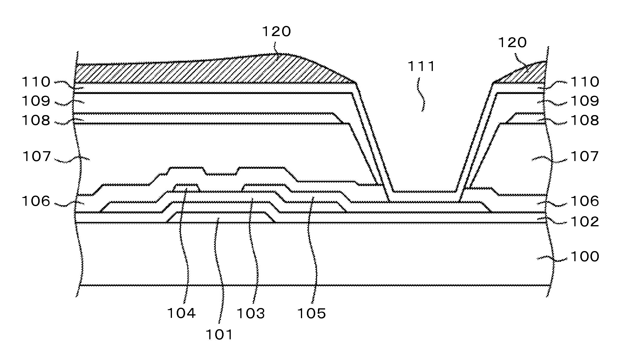
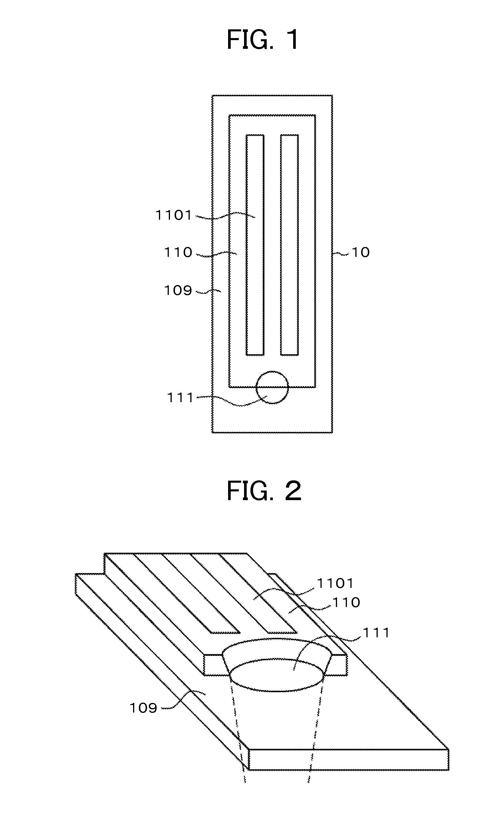
[0049]FIG. 1 depicts a pixel 10 according to the present invention. Referring to FIG. 1, a pixel electrode 110 having a slit 1101 is formed on an interlayer insulating film 109 made of SiN. A counter substrate not depicted is formed below the interlayer insulating film 109. If a signal voltage is applied to the pixel electrode 110, then electric lines of force are directed through the slit 1101 of the pixel electrode 110 to the underlying counter electrode. Thereupon, a transverse electric field is formed in a liquid crystal layer, and liquid crystal molecules are rotated by the transverse electric field. The transmittance of the liquid crystal is controlled thereby for each pixel 10 to form an image.

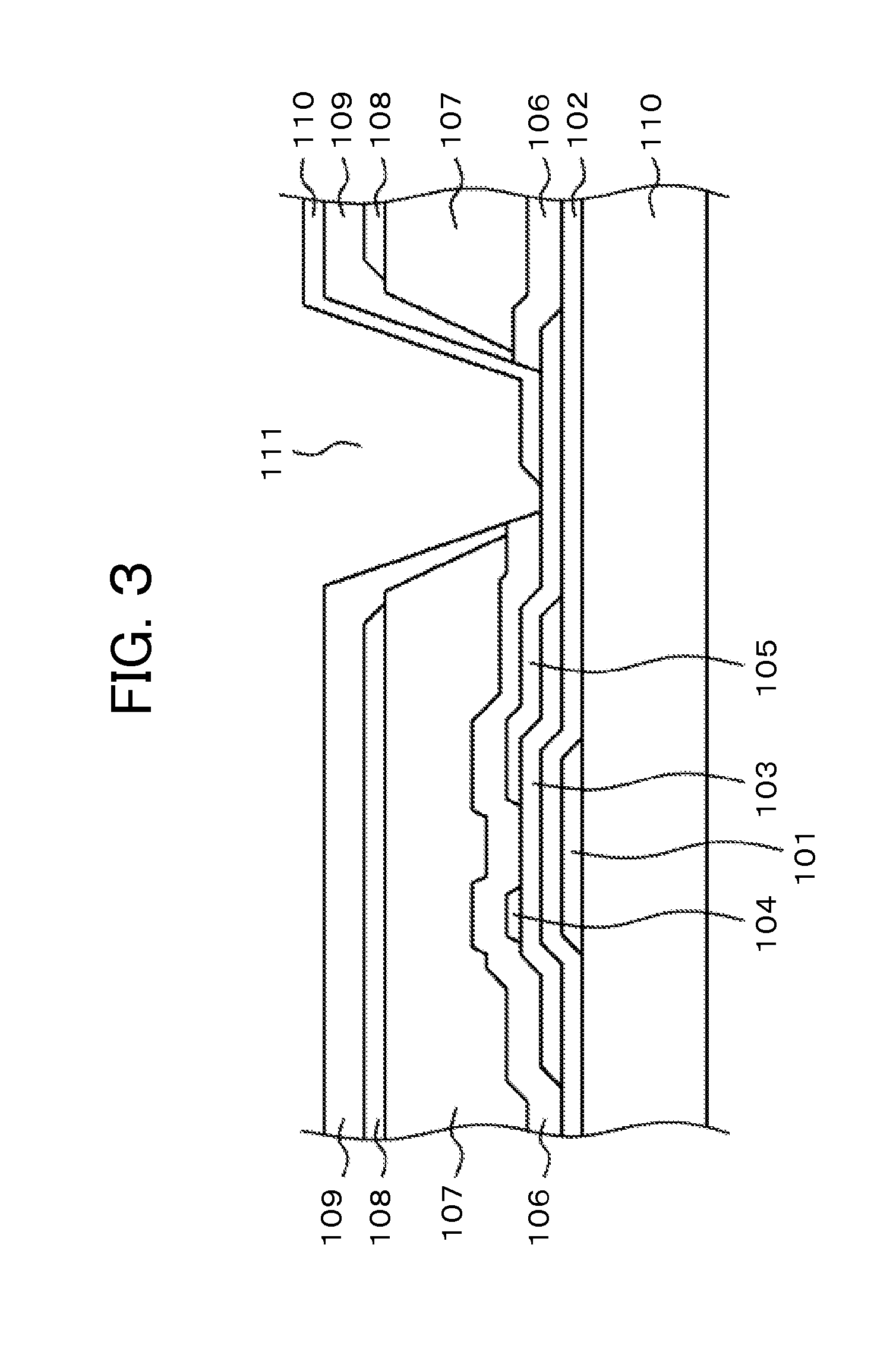
[0050]The pixel electrode 110 is connected to the source electrode of a TFT through a through-hole 111. However, the present invention is characterized in that the pixel electrode 110 does not cover the entire through-hole 111 and, on the outer side of the pixel, the pixel electrode 110...

embodiment 2

[0054]FIG. 4 is a top plan view of a pixel depicting a second embodiment of the present invention. A through-hole 111 has a large opening 1112 and a small opening 1111. The pixel in FIG. 4 is characterized in that the large opening 1112 of the through-hole 111 has an elliptical shape having a major axis in the longitudinal direction of the pixel. Accordingly, in the sectional shape of the through-hole 111, the taper angle of a cross section in the major axis direction of the pixel is smaller than the taper angle of a cross section in the minor axis direction of the pixel.

[0055]Further, FIG. 4 is characterized in that a slit 1101 of the pixel electrode 110 extends to the inner wall of the through-hole 111. Accordingly, on a periphery of the upper side of the through-hole 111, a step arising from the presence of the slit 1101 of the pixel electrode 110 is formed. An orientation film material flows readily into the through-hole from a starting point given by the step.

[0056]Further, the...

embodiment 3

[0059]FIG. 5 is a top plan view depicting a third embodiment of the present invention. The present embodiment is characterized in that a through-hole 111 has an elliptical shape having a major axis in the longitudinal direction of the pixel and besides a pixel electrode 110 is separated into a main pixel electrode having a slit 1101 and a sub pixel electrode disposed on the outer side of the pixel. A gap 112 is provided between the main pixel electrode and the sub pixel electrode.

[0060]On the major axis side of a large opening 1112 of the through-hole 111, the taper angle of the inner wall of the through-hole 111 is smaller. Further, on the major axis side of the large opening 1112 of the through-hole 111, ITO which configures the pixel electrode 110 does not exist, and SiN which configures an interlayer insulating film 109 is exposed. Further, at the gap 112 at which ITO does not exist, a step of the ITO is formed.

[0061]In particular, in the present embodiment, the pixel is structu...


PUM

PropertyMeasurementUnit
diameteraaaaaaaaaa
diameteraaaaaaaaaa
thickaaaaaaaaaa

Abstract

To take measures against the phenomenon of difficulty for the orientation film material to flow into the through-hole when the diameter of through-holes which connects the pixel electrode and the source electrode becomes small.An interlayer insulating film 109 made of SiN is formed on a counter electrode, and a pixel electrode 110 having a slit 1101 is formed on the interlayer insulating film 109. A through-hole 111 which connects the pixel electrode 110 and the source electrode of a TFT has a large opening on the upper side, a small opening on the lower side, and an inner wall extending between the large opening and the small opening. The pixel electrode 110 covers the through-hole 111 on an inner side of the pixel of the through-hole 111 but does not cover a periphery of the large opening of the through-hole on an outer side of the through-hole 111. Consequently, an orientation film material can easily flow from a starting point given by an end portion of the pixel electrode into the inside of the through-hole.

Description

CLAIM OF PRIORITY[0001]The present application claims priority from Japanese Patent Application JP 2013-238130 filed on Nov. 18, 2013, the content of which is hereby incorporated by reference into this application.BACKGROUND OF THE INVENTION[0002]1. Field of the Invention[0003]The present invention relates to a display device, and particularly to a liquid crystal display device which is small in decrease in transmittance and low in pixel defect rate even on a high definition screen.[0004]2. Description of the Related Art[0005]In a liquid crystal display device, liquid crystal is sandwiched between a thin film transistor (TFT) substrate and a counter substrate. The TFT substrate has pixels formed in a matrix thereon and each including a pixel electrode, a TFT and so forth. The counter substrate opposed to the TFT substrate has color filters formed at places thereof corresponding to the pixel electrodes of the TFT substrate. The transmittance of light by liquid crystal molecules is co...

Claims


Application Information

Patent Timeline
Patent Type & Authority Applications(United States)
IPC IPC(8): G02F1/1362G02F1/1333G02F1/1339G02F1/1368
CPCG02F1/136227G02F1/1368G02F1/133305G02F1/13394G02F1/133345G02F1/1337
Inventor HYODO, YOSUKETOMIOKA, YASUSHIKUNIMATSU, NOBORUSONODA, HIDEHIROIMANISHI, YASUOHIROTA, TAKENORI
Owner JAPAN DISPLAY INC
Learn More