Photodiode with a dark current suppression junction

a photodiode and suppression junction technology, applied in the field of photodiodes, can solve the problem of setting the low-light limit of the sensitivity of the photosensor produ

Active Publication Date: 2015-05-28
TEXAS INSTR INC
View PDF4 Cites 7 Cited by
  • Summary
  • Abstract
  • Description
  • Claims
  • Application Information

AI Technical Summary

Benefits of technology

[0004]Most photodiode processes use a single junction. In such a configuration, the dark current is the same as the reverse-bias leakage current of a simple pn junction diode. Specifically, the pn junction collects minority carriers that are thermally excited within a diffusion length of the junction.
[0005]The following presents a simplified summary in order to provide a basic understanding

Problems solved by technology

This sets the low-light limit of sensitivity of a photosensor product, p

Method used


Image

  • Photodiode with a dark current suppression junction
  • Photodiode with a dark current suppression junction
  • Photodiode with a dark current suppression junction

Examples


case 1 (

[0027Prior Art): Unshielded SNWELL Cathode

IC,n,1=qADnLnnp

case 2 (

[0028Prior Art): NBL-Shielded Cathode, Grounded Emitter

IC,n,2=qADnWBnpIC,n,1(LnWB)>IC,n,1

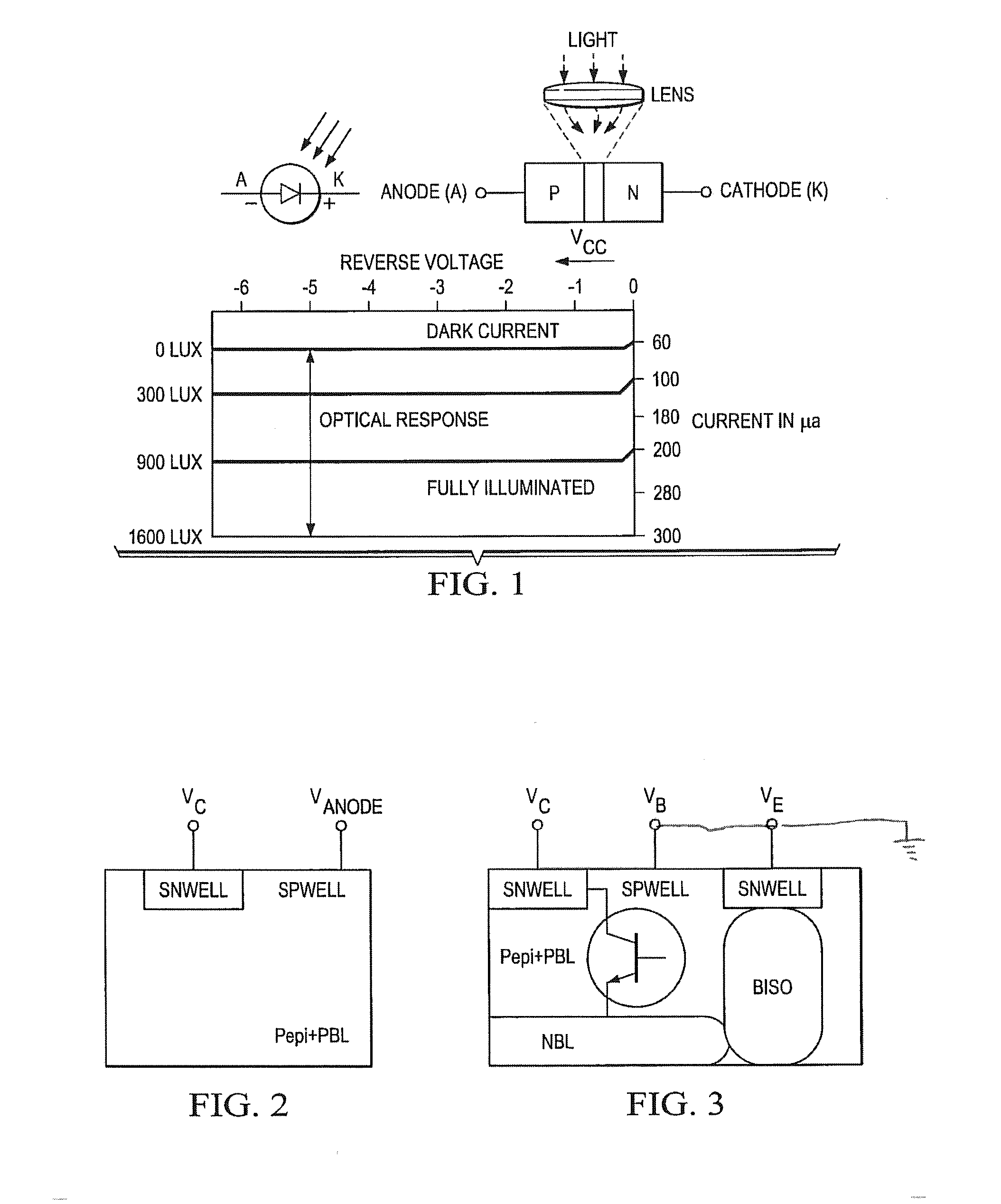
case 3 (first embodiment)

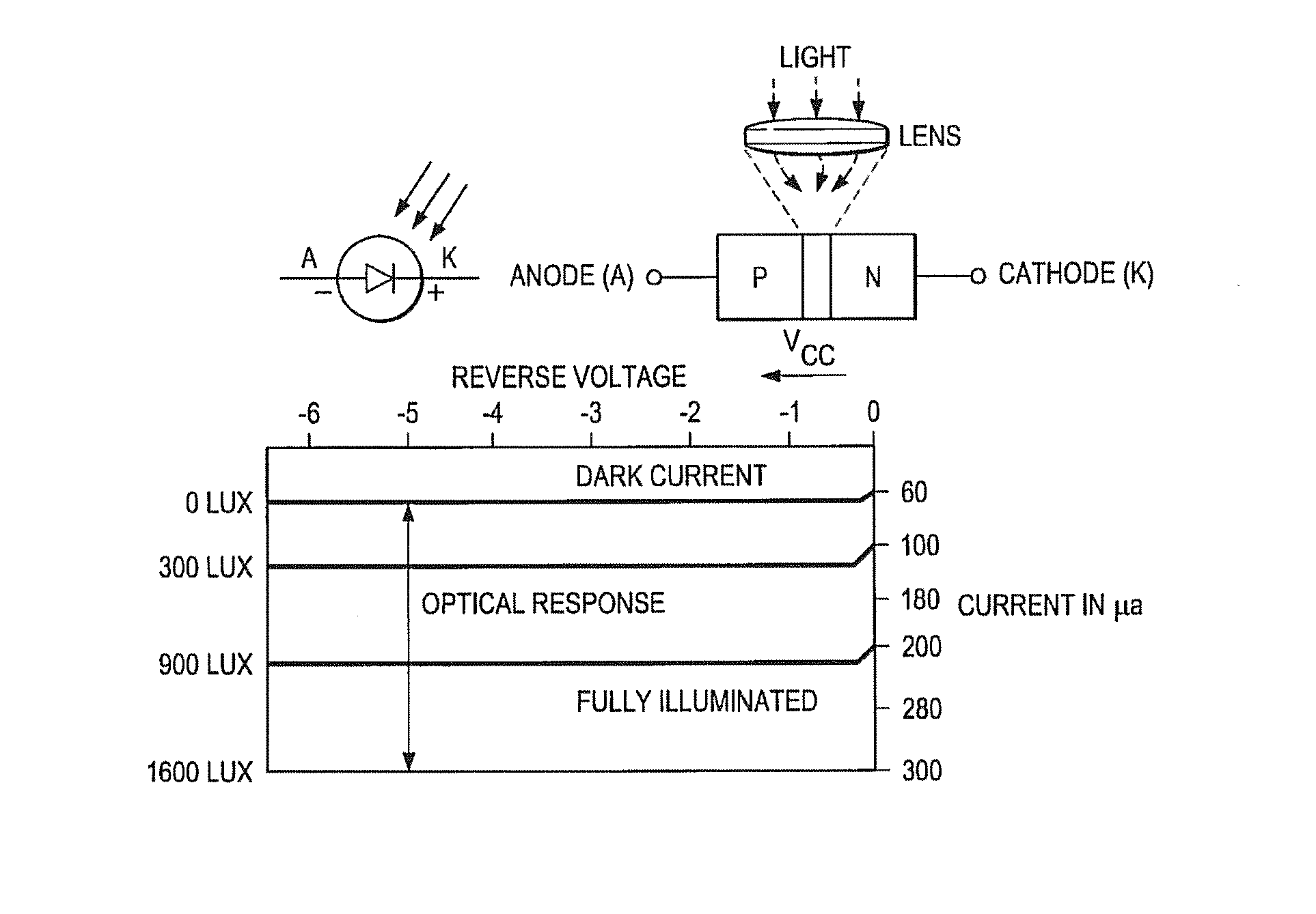
[0029] NBL-Shielded Cathode, Reverse Biased Emitter

IC,n,3=qADnLnnpWB2Ln=IC,n,2(12)(WBLn)2IC,n,2

[0030]Since it is possible to build an anode such that WB is much less than Ln (for example 10×), the present example constructed according to case 3 will have 100× lower dark current than a prior art photodiode constructed according to case 2 and 10× less dark current than the prior art single pn junction photodiode constructed according to case 1.

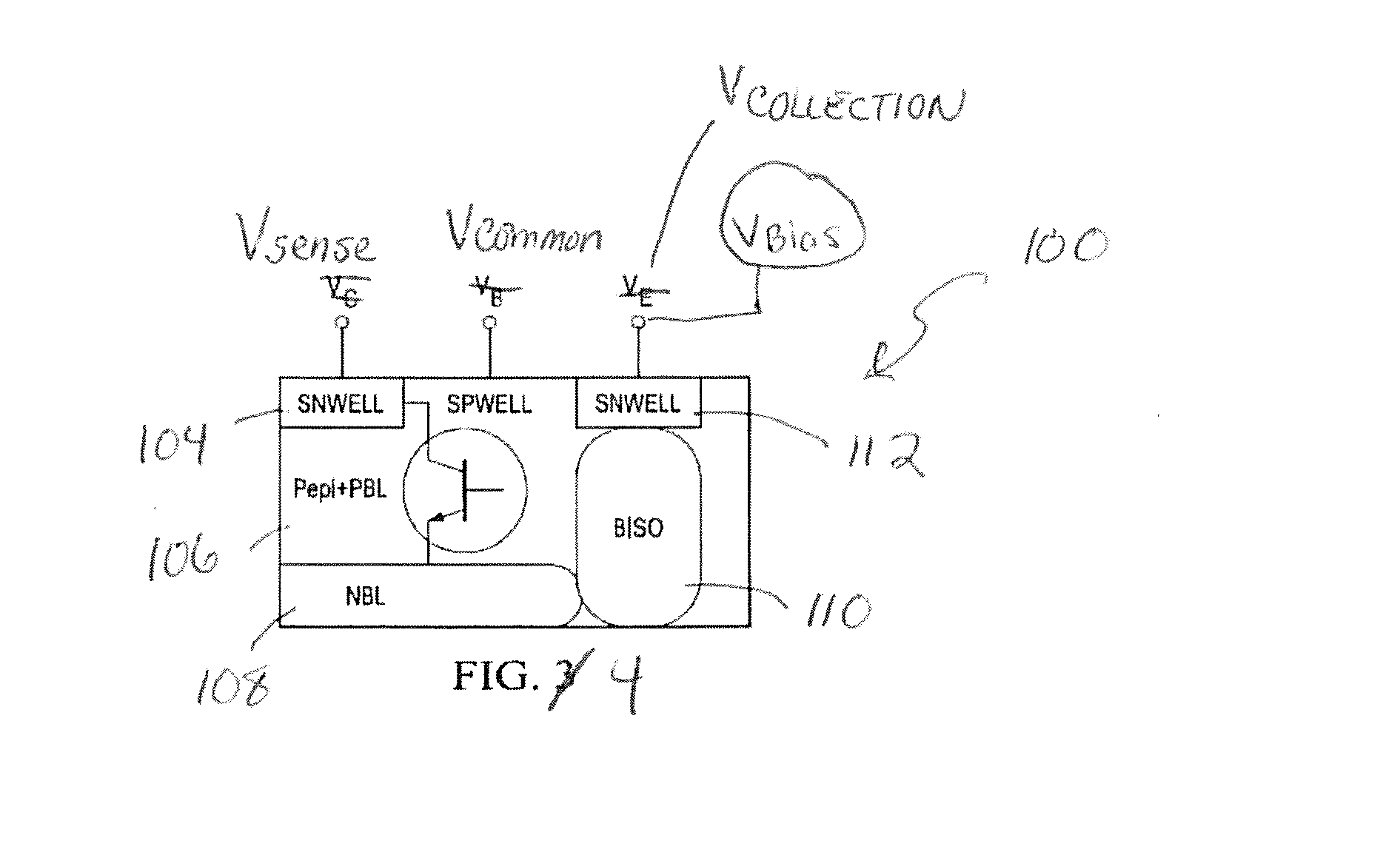
[0031]FIG. 5 shows a conceptual view of the NPN structure 100, with photons 102 illuminating the active region B and creating photoelectrons e″. In reality the photon illumination comes in from the surface of the silicon, so the photoelectrons are created in the SNWELL collector / cathode, the pepi base / anode B, the NBL emitter / shield, and the first epi / psub region. The “most important” photoelectrons are those produced in the SNWELL and pepi since all the rest are collected by the NBL and taken away from the signal path (which goes between anode ...


PUM


Abstract

This invention relates to field photodiodes based on PN junctions that suffer from dark current leakage. An NBL is added to prove a second PN junction with the anode. The second PN junction is reversed biased in order to remove dark current leakage. The present solution requires no additional masks or thin films steps relative to a conventional CMOS process flow.

Description

CROSS-REFERENCE TO RELATED APPLICATIONS[0001]This application claims the benefit of priority under U.S.C. §119(e) of U.S. Provisional Application 61 / 908,304 (Texas Instruments docket number TI-74240PS), filed Nov. 25, 2013 the contents of which are hereby incorporated by reference.FIELD OF THE INVENTION[0002]This invention relates to the field of photodiodes based on PN junctions. More particularly, this invention relates to field photodiodes based on PN junctions that suffer from dark current leakage.BACKGROUND OF THE INVENTION[0003]Photodiodes based on PN junctions suffer from dark current, which is essentially the normal PN junction reverse bias leakage current that will be detected in the absence of a light signal (See, FIG. 1). The dark current must be subtracted from the photodiode signal in order to sense the light signal intensity accurately. This sets the low-light limit of sensitivity of a photosensor product, particularly at high temperature where PN junction leakage is t...

Claims


Application Information

Patent Timeline
IPC IPC(8): H01L31/11H01L31/02H01L31/18
CPCH01L31/1105H01L31/02005H01L31/18
Inventor BASU, DEBARSHIEDWARDS, HENRY LITZMANNTRIFONOV, DIMITAR TRIFONOVDU, JOSH
Owner TEXAS INSTR INC
Why Eureka
Try Eureka