Clamped Avalanche Photodiode

Active Publication Date: 2016-07-28
LADARSYST INC
View PDF7 Cites 81 Cited by
  • Summary
  • Abstract
  • Description
  • Claims
  • Application Information

AI Technical Summary

Problems solved by technology

The electron or hole can accelerate again, as can the secondary electron or hole, and create more electron-hole pairs, resulting in an avalanche.

Method used


Image

  • Clamped Avalanche Photodiode
  • Clamped Avalanche Photodiode
  • Clamped Avalanche Photodiode

Examples


Embodiment Construction

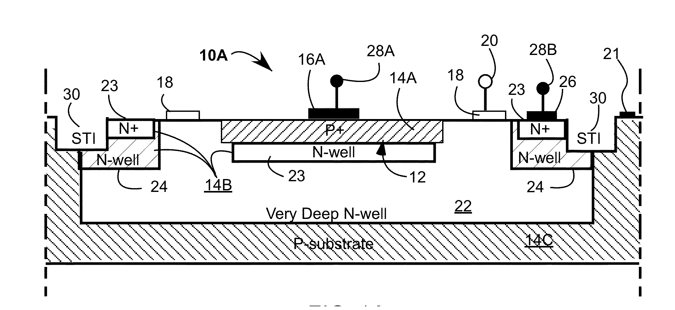
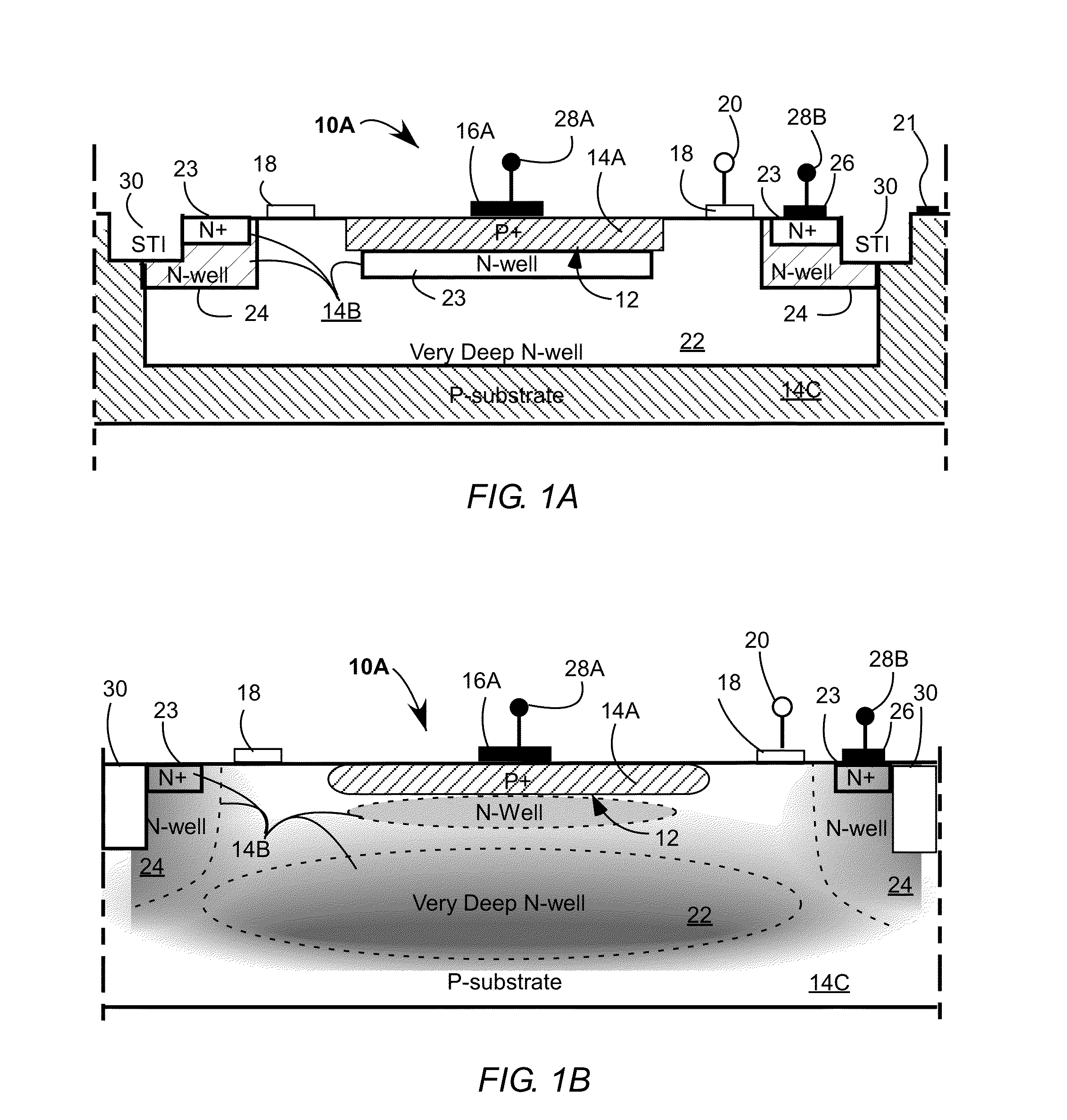
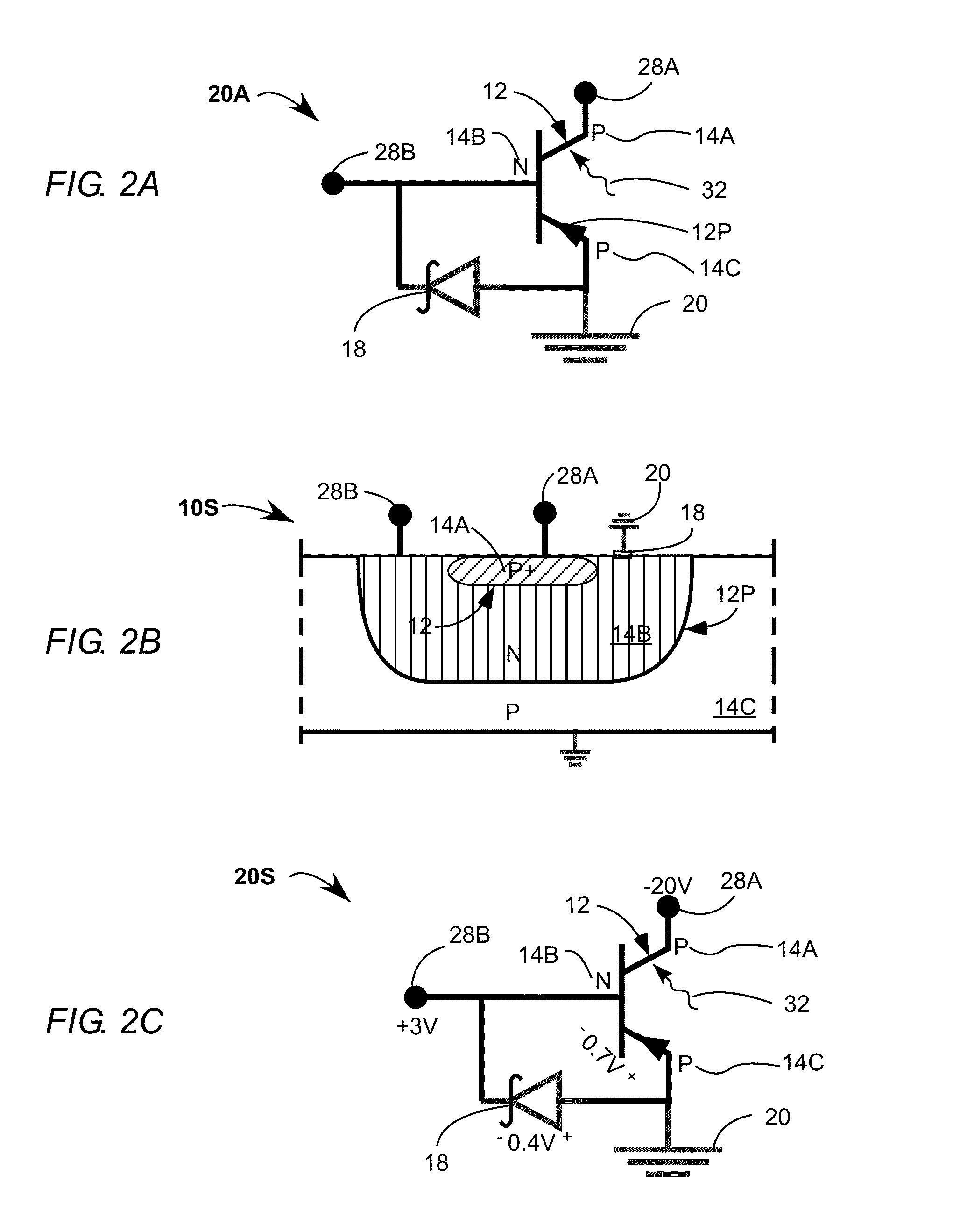
[0021]Referring now to the drawings, wherein like components are designated by like reference numerals. Devices and methods of manufacture are described further herein below.

[0022]FIG. 1A and FIG. 1B schematically illustrates a device 10A, an embodiment of the present disclosure. Device 10A is an avalanche photodiode device operated in Geiger-mode. FIG. 1A conceptually depicts the device. Rectangles refer and distinguish doping areas and regions, although such strict borders do not exist in actual devices. FIG. 1B depicts the areas and regions with dashed lines and concentration of N-type carriers as darker regions, depicting the device in a more accurate manner.

[0023]Device 10A comprises of a P-N junction 12, the P-N junction formed on a substrate by a first semiconductor region 14A and a second semiconductor region 14B. A third semiconductor region 14C is in contact with the second region, is not in contact with first semiconductor region 14A, and is the same semiconductor-type as...


PUM


Abstract

An avalanche photodiode device operated in Geiger-mode, the device comprising a P-N junction formed on a substrate with a first semiconductor region and a second semiconductor region with an anode and cathode. The device further comprising a third semiconductor region, the third semiconductor region in physical contact with the second region, not in physical contact with the first region, and being the same semiconductor-type as the first semiconductor region. Additionally comprising a diode on the second semiconductor region and having a turn-on voltage than the P-N junction.

Description

RELATED APPLICATIONS[0001]This application claims benefit to U.S. Provisional Application No. 62 / 108,198 filed on Jan. 27, 2015.TECHNICAL FIELD OF THE DISCLOSURE[0002]The present disclosure relates in general to photonic detectors. This disclosure relates in particular to avalanche photodiodes operated in Geiger-mode, also known as single-photon avalanche diodes (SPAD).DISCUSSION OF BACKGROUND ART[0003]Avalanche Photodiodes are highly sensitive photonic detectors. Avalanche photodiodes are reverse biased solid state devices with high electric field. When a photon of sufficient energy is absorbed in the device where the field exists, an electron-hole pair is generated under the influence of this field, resulting in photocurrent. If this field is sufficiently high, one of the carriers accelerates and gains sufficient energy to collide with the crystal lattice and generate another electron-hole pair. This process is known as impact ionization. The electron or hole can accelerate again,...

Claims


Application Information

Patent Timeline
Patent Type & Authority Applications(United States)
IPC IPC(8): H01L31/107H01L29/872H01L27/144
CPCH01L31/107H01L29/872H01L27/1443H01L27/1446
Inventor DHULLA, VINITMILLER, DRAKEFORBES, LEONARD
Owner LADARSYST INC
Why Eureka
Try Eureka