One-chip micro-integrated optoelectronic sensor

a technology of optoelectronic sensor and micro-integration, which is applied in the field of optical measurements, can solve the problem of not providing a single technological process for sensor fabrication, and achieve the effect of reducing the number of manufacturing steps

Inactive Publication Date: 2005-04-19
HOUSTON UNIV OF
View PDF16 Cites 86 Cited by
  • Summary
  • Abstract
  • Description
  • Claims
  • Application Information

AI Technical Summary

Benefits of technology

[0024]The employment of pre-breakdown avalanche electroluminescense, which allows emission of light with energies higher than the semiconductor's band gap, allows spectral matching of the emission and photosensitivity spectra from diode structures based on the same semiconductor material. It also allow emission to extend into the UV range and makes possible emission at two different ranges from the same junction (pre-breakdown avalanche at a reverse bias and recombination at a forward bias.

Problems solved by technology

The '169 patent requires the integration of at least one optical waveguide in the sensor to measure one or more variables and does not provide a method of sensor fabrication requiring only a single technological process.

Method used


Image

  • One-chip micro-integrated optoelectronic sensor
  • One-chip micro-integrated optoelectronic sensor
  • One-chip micro-integrated optoelectronic sensor

Examples


Embodiment Construction

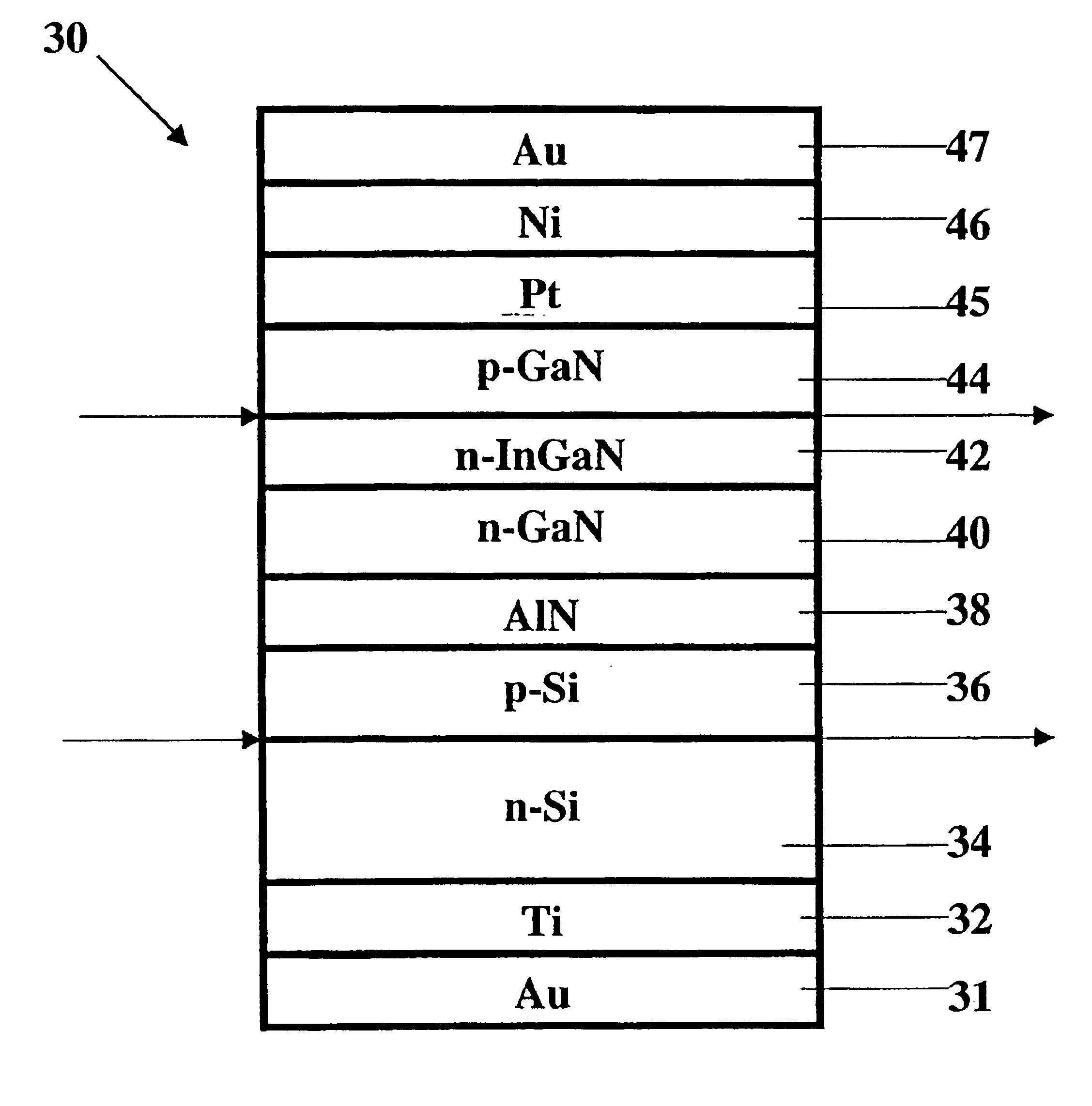
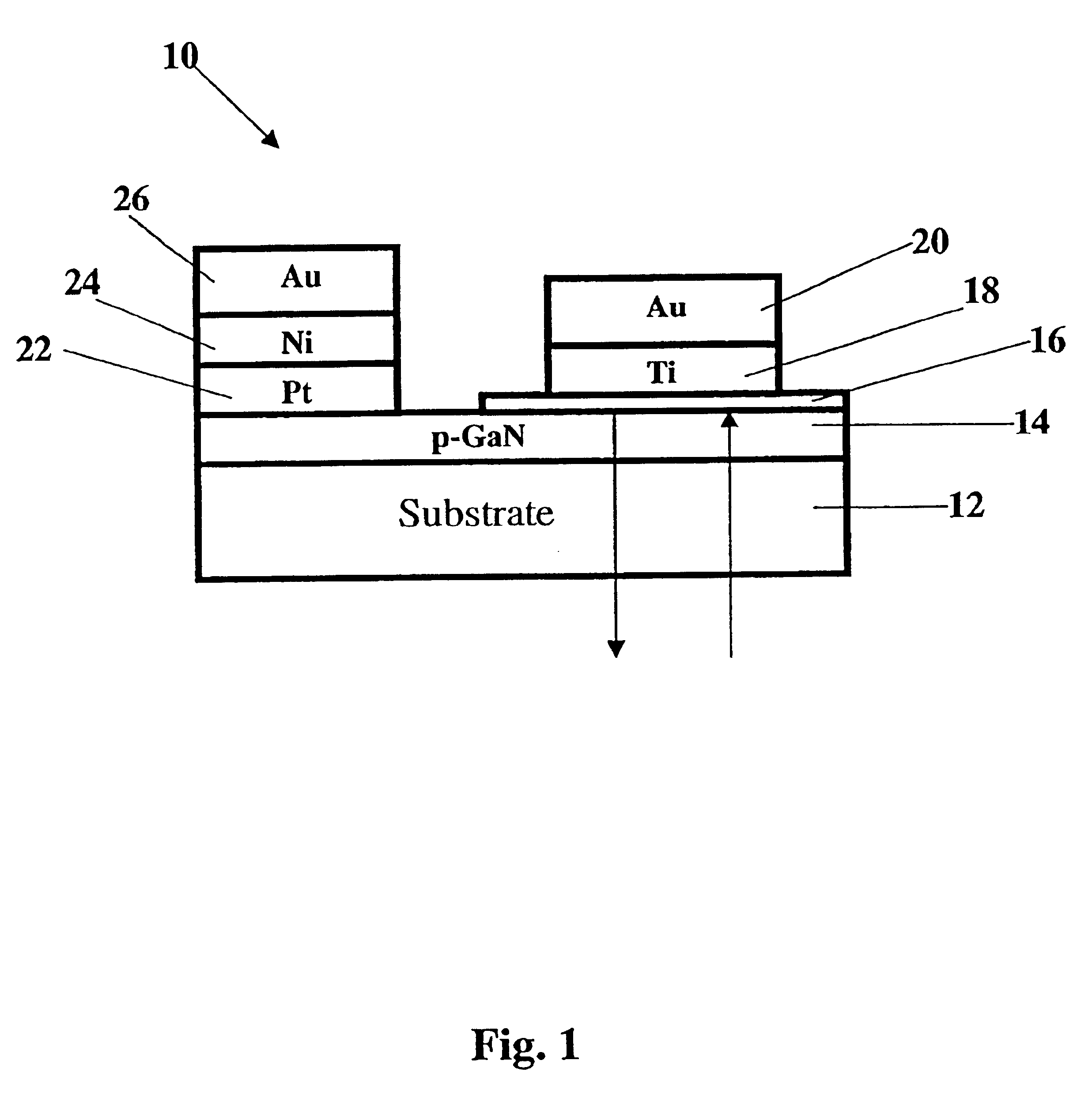
[0030]One embodiment of a one-chip micro-integrated optoelectronic sensor is shown generally at 10 in FIG. 1. As indicated by arrows representing light rays in the figure, structure 10 provides an optical emission source (LED) or a photodetector (PD) on a single substrate or chip. The device is fabricated on optically transparent semiconductor layer 14 and optically transparent substrate 12. Similar optoelectronic properties, device structures, and operation principles for the disclosed sensor can be achieved on several optically transparent semiconductor materials grown on optically transparent substrates. Materials that can be used for semiconductor layer 14 include in the near UV / visible range of the spectrum any of the III-V nitride compounds, zinc oxide (ZnO), silicon carbide (SiC), tin oxide (SnO2), indium oxide (In2O3) and diamond. Materials that can be used for transparent substrate 12 include sapphire, quartz and optically transparent glasses. Only the characteristics of st...


PUM


Abstract

This disclosure describes one-chip micro-integrated optoelectronic sensors and methods for fabricating and using the same. The sensors may include an optical emission source, optical filter and a photodetector fabricated on the same transparent substrate using the same technological processes. Optical emission may occur when a bias voltage is applied across a metal-insulator-semiconductor Schottky contact or a p-n junction. The photodetector may be a Schottky contact or a p-n junction in a semiconductor. Some sensors can be fabricated on optically transparent substrate and employ back-side illumination. In the other sensors provided, the substrate is not transparent and emission occurs from the edge of a p-n junction or through a transparent electrode. The sensors may be used to measure optical absorption, optical reflection, scattering or fluorescence. The sensors may be fabricated and operated to provide a selected spectrum of light emitted and a multi-quantum well heterostructure may be fabricated to filter light reaching the photodetector.

Description

CROSS-REFERENCE TO RELATED APPLICATIONS[0001]This patent application is a division of, and claims priority to, commonly owned U.S. patent application Ser. No. 09 / 738,728, filed Dec. 15, 2000, entitled “One-Chip Micro-Integrated Optoelectronic Sensor,” by David Starikov, Igor Berishev and Abdelhak Bensaoula, which will issue to U.S. Pat. No. 6,608,360 on Aug. 19, 2003, and which is incorporated herein by reference for all purposes.[0002]This patent application is also related to commonly owned U.S. patent application Ser. No. 10 / 621,545, filed Jul. 17, 2003, entitled “Measuring Spectral Characteristics Using Filterless Solid State Semiconductor Components,” by David Starikov and Abdelhak Bensaoula, which itself is a continuation-in-part application of the above-referenced and commonly owned U.S. patent application Ser. No. 09 / 738,728.FIELD OF THE INVENTION[0003]This invention generally relates to optical measurements. More particularly, a light-emitting diode and a photodiode formed ...

Claims


Application Information

Patent Timeline
Patent Type & Authority Patents(United States)
IPC IPC(8): H01L29/66H01L27/15H01L31/0264H01L31/0312H01L29/861H01L31/108H01L31/173H01L31/18
CPCH01L31/108H01L31/1852H01L31/173Y02E10/544Y02P70/50
Inventor STARIKOV, DAVIDBERISHEV, IGORBENSAOULA, ABDELHAK
Owner HOUSTON UNIV OF
Why Eureka
Try Eureka