Nanowire Array-Based Light Emitting Diodes and Lasers

a technology of light-emitting diodes and nanowires, applied in the direction of lasers, semiconductor lasers, material nanotechnology, etc., can solve the problems of limited directionality, inability to dim, slow starting, etc., and achieve low threshold injection lasers, low lasing threshold reduction, high efficiency

Inactive Publication Date: 2011-07-07
RGT UNIV OF CALIFORNIA
View PDF11 Cites 76 Cited by
  • Summary
  • Abstract
  • Description
  • Claims
  • Application Information

AI Technical Summary

Benefits of technology

[0013]Nanowires form natural Fabry-Perot cavities so that amplified spontaneous emission (ASE) can be achieved. In one embodiment, superlattices are used to define distributed Bragg reflector (DBR) structures in nanowires to reduce the lasing threshold. Growth of axial heterostructure nanowires (superlattices) along the length of the nanowire and the nanowire arrays allow high efficiency, low threshold injection lasers. The nanowire array lasers can also be fabricated by lithographically etching down from a layer structure, such as a vertical-cavity surface-emitting laser (VCSEL), into nanoscale wire arrays.
[0014]In a preferred embodiment, ZnO nanowires and core / shell nanowire arrays are used to manufacture LEDs and laser diodes. Nanowires formed from ZnO doped with phosphors or un-doped, or ZnO alloys, including MgZnO, ZnBeO, ZnCdO, can be used as active building blocks for light emitting diodes, providing for low cost manufacturing of LEDs.
[0015]Compared to planar thin film LEDs, nanowires have a large surface area-to-volume ratio, which is proportional to the diameter of the nanowire. The large total surface area provides an enlarged carrier injection p / n junction area in which the electrons and holes recombine and emit photons. Heterostructures and superlattices grown along the lengths of the nanowires, or formed radially across the nanowires, allow the confinement of photons in the quantum well to enhance the efficiency and as well as provide for color tuning
[0016]The nanowire array geometry is typically perfectly vertical, or within a small range of variations from vertical, relative to the substrate. The small nanowire diameters minimize or eliminate the total internal reflection that normally occurs with existing planar thin film LEDs, further enhancing light extraction efficiency.
[0017]Single crystal ZnO nanowire growth is not limited by lattice matched substrates, and therefore can grow virtually from any substrate, unlike their thin film counterparts. GaN-based thin film LEDs require expensive substrates such as SiC or sapphire, and there can still be large lattice mismatch between the GaN and the substrate, such that defect-free thin film is hard to achieve. These defects tend to limit LED efficiency. ZnO thin film LEDs show promise because of the availability of inexpensive lattice matched ZnO substrate, and has the further advantage that no toxic precursors are required. ZnO nanowires can be easily synthesized using solution-based methods, which could further bring down the cost of LEDs fabricated using ZnO nanowires.

Problems solved by technology

While the push to adopt compact fluorescent lighting (CFL) has achieved some progress toward the goals of energy efficiency, there are several drawbacks to the CFL bulbs, which include slow starting, inability to dim, limited directionality, and their use of small amounts of mercury, which in some states requires discarded bulbs to be treated as hazardous waste.
A variety of white LEDs are currently available commercially, however they cannot yet compete with traditional light sources on the basis of performance or cost.
However, similar to other wide bandgap semiconductors, such as GaN, unintentionally doped ZnO is intrinsically n-type and obtaining p-type doping has proven extremely challenging.

Method used


Image

  • Nanowire Array-Based Light Emitting Diodes and Lasers
  • Nanowire Array-Based Light Emitting Diodes and Lasers
  • Nanowire Array-Based Light Emitting Diodes and Lasers

Examples


Embodiment Construction

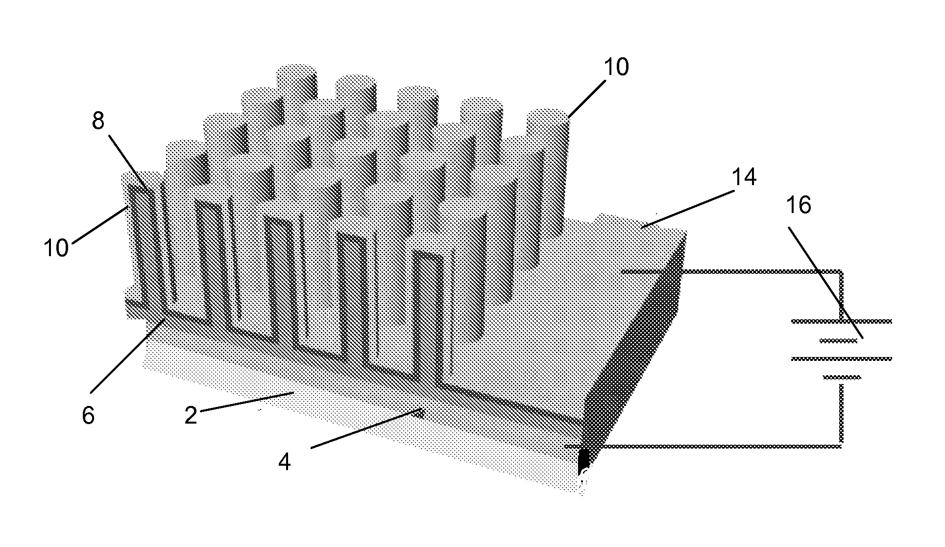
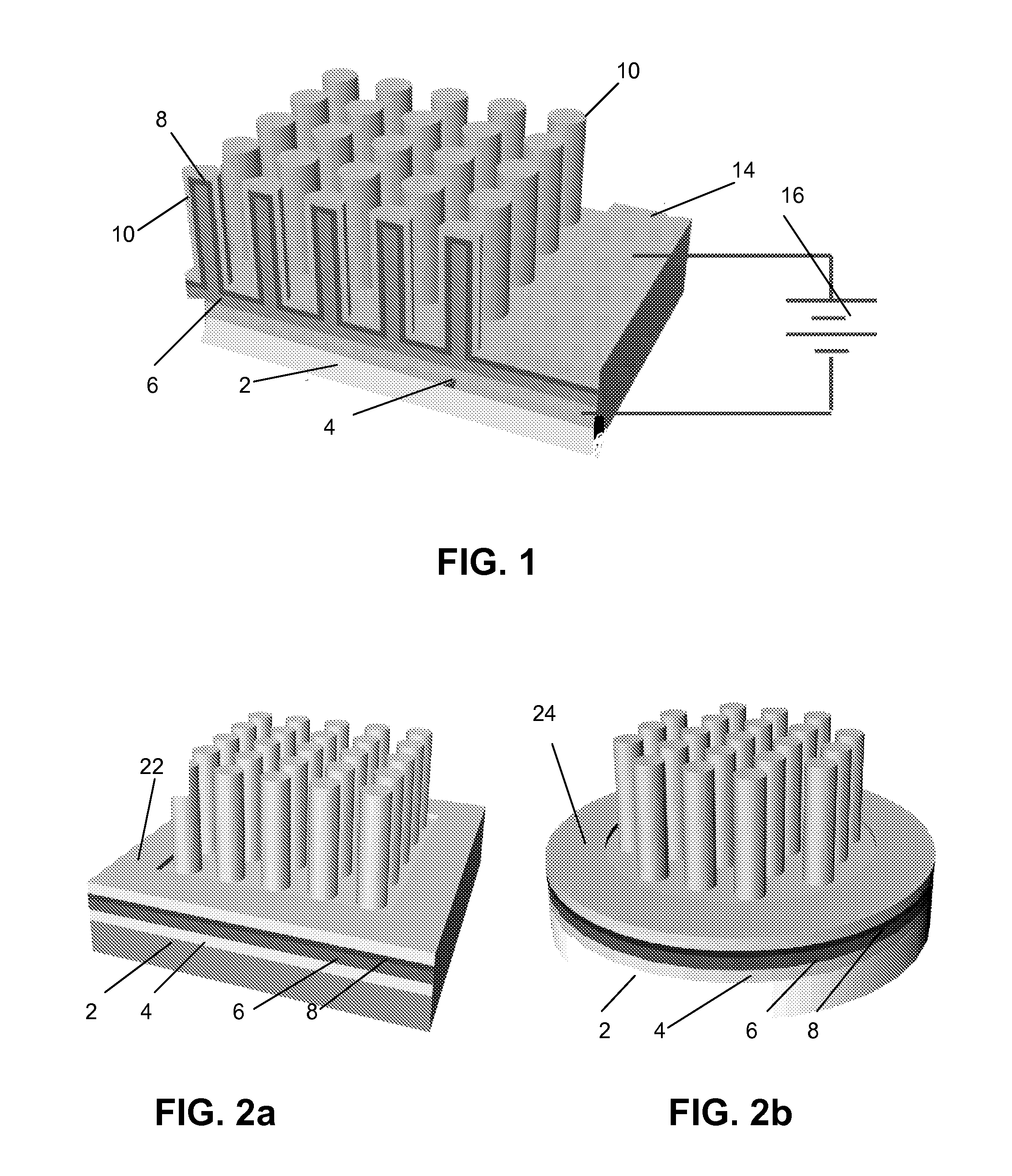
[0027]According to the present invention, semiconductor nanowire arrays are used to replace the conventional layer design for fabrication of LEDs and laser diodes. In one embodiment, core-shell nanowire arrays are formed on a conducting substrate using known nanowire growth techniques, including Chemical Vapor Deposition (CVD), Metal Organic Chemical Vapor Deposition (MOCVD), Molecular and Chemical Beam Epitaxy (CBE and MBE), solution syntheses, and template-assisted electrochemical syntheses. The conducting substrates can be ITO (indium tin oxide), FTO (fluorine-doped tin oxide), tin oxide, zinc oxide, degenerated doped Si, metals, or other similar materials. Where the growth technique is solution-based, the nanowires can also be formed on a metal coated substrates that can later serve as an electrode.

[0028]The nanowires can be formed from III-V or II-VI compound semiconductors, such as AlInGa, ZnO, and alloys thereof, such as AlxInyGa(1-x-y)PzAs(1-z), AlxInyGa(1-x-y)PzAs(1-z):N (d...


PUM

PropertyMeasurementUnit
Correlated Color Temperaturesaaaaaaaaaa
diametersaaaaaaaaaa

Abstract

Semiconductor nanowire arrays are used to replace the conventional planar layered construction for fabrication of LEDs and laser diodes. The nanowire arrays are formed from III-V or II-VI compound semiconductors on a conducting substrate. For fabrication of the device, an electrode layer is deposited on the substrate, a core material of one of a p-type and n-type compound semiconductor material is formed on top of the electrode as a planar base with a plurality of nanowires extending substantially vertically therefrom. A shell material of the other of the p-type and n-type compound semiconductor material is formed over an outer surface of the core material so that a p-n junction is formed across the planar base and over each of the plurality of nanowires. An electrode coating is formed an outer surface of the shell material for providing electrical contact to a current source. Heterostructures and superlattices grown along the lengths of the nanowires allow the confinement of photons in the quantum well to enhance the efficiency and as well as color tuning.

Description

RELATED APPLICATIONS[0001]This application claims the priority of U.S. Provisional Application No. 60 / 870,559 filed Dec. 18, 2006, the disclosure of which is incorporated herein by reference in its entirety.GOVERNMENT RIGHTS[0002]Pursuant to 35 U.S.C. §202(c), it is hereby acknowledged that the U.S. government has certain rights in the invention described herein, which invention was made in part with funds from the Office of Naval Research (ONR), Grant No. 14-05-1-0149, and National Science Foundation, Grant No. ECS-0506902.BACKGROUND OF THE INVENTION[0003]Increasing environmental awareness relating to global climate change and the desire to reduce dependence on imported fuel sources have helped drive efforts to develop technologies that enable more efficient usage of electrical energy. In the United States, the amount of electricity consumed for lighting is significant, accounting for around 18-20% of the total energy usage in buildings. While the push to adopt compact fluorescent ...

Claims


Application Information

Patent Timeline
Patent Type & Authority Applications(United States)
IPC IPC(8): H01L33/06H01L33/30H01L33/28B82Y40/00B82Y99/00H01L33/18H01L33/24
CPCB82Y20/00B82Y30/00H01L33/18H01S5/423H01S5/1042H01S5/183H01L33/24
Inventor WANG, DELIBAO, XINYUXIANG, BINSOCI, CESAREAPLIN, DAVID
Owner RGT UNIV OF CALIFORNIA
Why Eureka
Try Eureka