Wavelength tunable laser

a wavelength-tunable laser and wavelength-tunable technology, applied in the field of optical communication, can solve the problems of large device size, large device inventory, low output power and very limited wavelength tuning range, etc., and achieve the effects of broad band wavelength tuning, high speed, and simple mechanical structur

Inactive Publication Date: 2005-05-10
MIND FUSION LLC +1
View PDF23 Cites 57 Cited by
  • Summary
  • Abstract
  • Description
  • Claims
  • Application Information

AI Technical Summary

Benefits of technology

[0007]The present invention is directed to an improved tunable wavelength light source for use in optical communications systems that facilitates high speed, broad band wavelength tuning, is mechanically simple, scalcable and reliable, and facilitates monolithic integration of optical components. The novel wavelength tunable light source of the present invention preferably comprises a semiconductor laser diode optically coupled to a tunable wavelength selective external cavity. Preferably, the external cavity comprises a waveguide-coupled optical resonator that includes an optical resonator, or multiple optical resonators, either horizontally or vertically coupled to adjacent semiconductor waveguides. The optical resonator, which is preferably formed from electro-optic materials, primarily functions as a wavelength selector and can be in the form of a disk, ring or other closed cavity geometries. In operation, light signal emissions from one end of the semiconductor laser may be coupled into a first waveguide using an optical lens or butt-joint method, and then transferred to a second waveguide through evanescent coupling between the waveguides and the optical resonator when the wavelength of the light signal is at a resonance frequency of the resonator. A mirror system or high reflection coating at the end of the second waveguide reflects the light signal back into the system. A closed optical cavity is realized as a result.
[0008]Lasing can be achieved in the light source of the present invention when the optical gain overcomes the optical loss in the closed cavity for a certain resonance wavelength. The resonance wavelength is preferably tunable by changing the resonance condition of the optical resonator through current or reversed biased voltage. For a given material and structure, the wavelength tunable range tends to be determinable by the size of the resonator. The use of multiple optical resonators advantageously tends to reduce the lasing threshold and tends to provide higher power output.
[0009]When compared to traditional ECL designs, the wavelength tunable laser of the present invention tends to possess several advantages. For instance, the present invention tends to be smaller in size because of its use of compact waveguide-coupled optical resonators as the external cavity. The tunable laser of the present invention also tends to have much faster tuning speeds because the tuning mechanisms use electro-optic effects or carrier effects instead of thermal or MEMS effects. Lastly, the semiconductor laser diode and the optical resonators forming the tunable laser of the present invention may be fabricated on the same substrate and, thus, facilitate monolithic integration.
[0013]A significant advantage of the tunable laser of the present invention, as compared to other ECL designs, is that monolithic integration tends to be possible. For example, the laser diode is fabricated first on an InP substrate. The optical resonators and coupling waveguides are then fabricated on the same substrate by using regrowth methods and other standard semiconductor fabrication processes. The emission of the laser diode is coupled into the first coupling waveguide through butt-joint methodology. In the same way, other optical devices can be integrated onto the same substrate and more complex functions can be realized. For example, an electro-absorption modulator may be fabricated right after the tunable laser wherein the output from the tunable laser may be modulated or another waveguide-coupled optical resonator may be coupled to the outputs from different tunable lasers to multiplex these outputs.

Problems solved by technology

In order to fully implement a DWDM system with thousands of channels under this wavelength-fixed scheme, service providers in the telecom industry face huge inventory, complexity, and cost problems because of the large number of laser sources and accessories needed, as well as the need for backup lasers and spare parts.
Although DFB lasers are well behaved and very reliable, they have the disadvantages of low output power and very limited wavelength tuning range (i.e., a range of about 5.0 nm).
DBR lasers have some advantages such as fast tuning speed, relatively large tuning range (about 40 nm), but suffer drawbacks of wavelength instability, broad linewidth, and large device size.
The use of MEMS tends to limit the tuning speed of the device within the microsecond range.
However, the main disadvantage of VCSELs is that they tend to have low output power (i.e., on the order of about hundreds of microwatts or lower).
Another disadvantage of traditional VCSELs is their operational wavelengths are limited to short wavelengths of about 850 nm to about 1300 nm.
However, most of current ECLs are very large, costly, sensitive to environmental changes, and operate with a slow tuning speed on the order of milliseconds.
In addition, current ECL designs tend not to be applicable to large-scaled integration.

Method used


Image

  • Wavelength tunable laser
  • Wavelength tunable laser
  • Wavelength tunable laser

Examples


Embodiment Construction

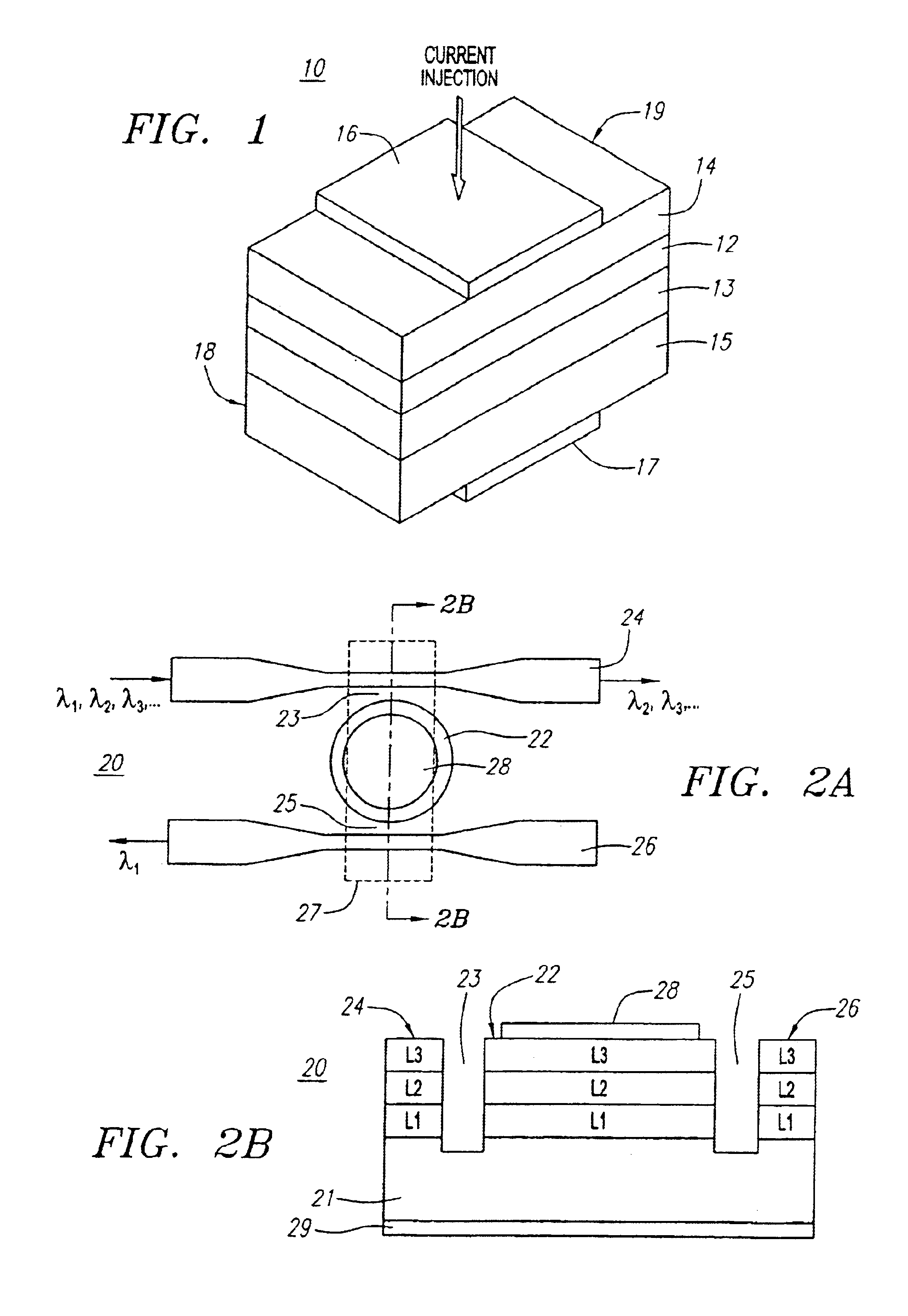
[0053]Referring in detail to the figures, a wavelength tunable laser of the present invention, as shown, combines a semiconductor laser diode with a waveguide-coupled optical resonator. The waveguide-coupled optical resonator serves as a wavelength selective, external cavity to realize a tunable laser by applying voltage or injecting current to change the resonance wavelength of the resonator(s).

[0054]Turning to FIG. 1, a multi-layer semiconductor wafer structure of a laser diode 10 of the present invention is shown. The laser diode 10 preferably comprises an active or guiding layer 12 sandwiched between two cladding layers 13 and 14 on a substrate 15. The active layer (guiding) 12 is preferably non-doped or insulated and has a higher refractive index (n) and a smaller bandgap than the two cladding layers 13 and 14. The two cladding layers 13 and 14 are preferably highly doped with either n-type or p-type doping in order to reduce contact resistance. The substrate 15 is preferably m...


PUM


Abstract

A wavelength tunable laser comprising a laser diode and a closed external cavity formed by one or more optical resonators either horizontally or vertically coupled to adjacent waveguides. The optical resonator primarily functions as a wavelength selector and may be in the form of disk, ring or other closed cavity geometries. The emission from one end of the laser diode is coupled into the first waveguide using optical lens or butt-joint method and transferred to the second waveguide through evanescent coupling between the waveguides and optical resonator. A mirror system or high reflection coating at the end of the second waveguide reflects the light backwards into the system resulting in a closed optical cavity. Lasing can be achieved when the optical gain overcomes the optical loss in this closed cavity for a certain resonance wavelength which is tunable by changing the resonance condition of the optical resonator through reversed biased voltage or current injection. Multiple optical resonators may be used to reduce the lasing threshold and provide higher power output. With monolithic integration, more optical devices can be integrated with the tunable laser into the same substrate to produce optical devices that are capable of more complex functions, such as tunable transmitters or waveguide buses.

Description

FIELD OF THE INVENTION[0001]The present invention relates to the field of optical communications and more particularly, to a light source with tunable wavelength for use in optical communications systems.BACKGROUND OF THE INVENTION[0002]The rapid growth of Internet data traffic has driven current fiber optic networks to a new stage where much broader bandwidth and higher capacity are required. Dense wavelength division multiplexed (DWDM) systems with narrow channel spacing and low crosstalk have proven to be a promising solution. Generally in a DWDM system, each channel is represented by a fixed wavelength from a wavelength-fixed laser source and all the different channels are sent into the same optical fiber and transmitted to a receiver end. In order to fully implement a DWDM system with thousands of channels under this wavelength-fixed scheme, service providers in the telecom industry face huge inventory, complexity, and cost problems because of the large number of laser sources ...

Claims


Application Information

Patent Timeline
Patent Type & Authority Patents(United States)
IPC IPC(8): H01S5/00H01S5/14H01S5/10
CPCH01S5/141H01S5/1032H01S5/1071H01S5/142H01S5/1075
Inventor MA, YONG
Owner MIND FUSION LLC
Why Eureka
Try Eureka