Reduction of Charging Induced Damage in Photolithography Wet Process

a technology of photolithography and wet process, applied in the field of semiconductor/solid-state device details, semiconductor devices, capacitors, etc., can solve the problems of damage already occurring in the underlying material (e.g., substrate), irreparable damage of the underlying substrate, and inability to repair. to achieve the effect of increasing the sticking of surface particles

Inactive Publication Date: 2015-06-04
CYPRESS SEMICON CORP
View PDF5 Cites 0 Cited by
  • Summary
  • Abstract
  • Description
  • Claims
  • Application Information

AI Technical Summary

Benefits of technology

[0008]In an embodiment of the present invention, the underlying cause was determined to be a substantial but undetected discharge that occurs in dielectric films in a certain thickness range while being patterned by lithography. The damage resulting from the undetected discharge is irreparable damage of the underlying substrate. Thus, even if the dielectric film is subsequently removed (e.g., a sacrificial oxide layer) and other layers take its place, the damage has already occurred in the underlying material (e.g., substrate) and cannot be repaired. In addition, the charge on the wafer surface also increases the sticking of surface particles due to electrostatic attraction.

Problems solved by technology

The damage resulting from the undetected discharge is irreparable damage of the underlying substrate.
Thus, even if the dielectric film is subsequently removed (e.g., a sacrificial oxide layer) and other layers take its place, the damage has already occurred in the underlying material (e.g., substrate) and cannot be repaired.
In addition, the charge on the wafer surface also increases the sticking of surface particles due to electrostatic attraction.

Method used


Image

  • Reduction of Charging Induced Damage in Photolithography Wet Process
  • Reduction of Charging Induced Damage in Photolithography Wet Process
  • Reduction of Charging Induced Damage in Photolithography Wet Process

Examples


Embodiment Construction

[0021]This specification discloses one or more embodiments that incorporate the features of this invention. The disclosed embodiment(s) merely exemplify the invention. The scope of the invention is not limited to the disclosed embodiment(s). The invention is defined by the claims appended hereto.

[0022]The embodiment(s) described, and references in the specification to “one embodiment,”“an embodiment,”“an example embodiment,” etc., indicate that the embodiment(s) described may include a particular feature, structure, or characteristic, but every embodiment may not necessarily include the particular feature, structure, or characteristic. Moreover, such phrases are not necessarily referring to the same embodiment. Further, when a particular feature, structure, or characteristic is described in connection with an embodiment, it is understood that it is within the knowledge of one skilled in the art to effect such feature, structure, or characteristic in connection with other embodiments...


PUM


Abstract

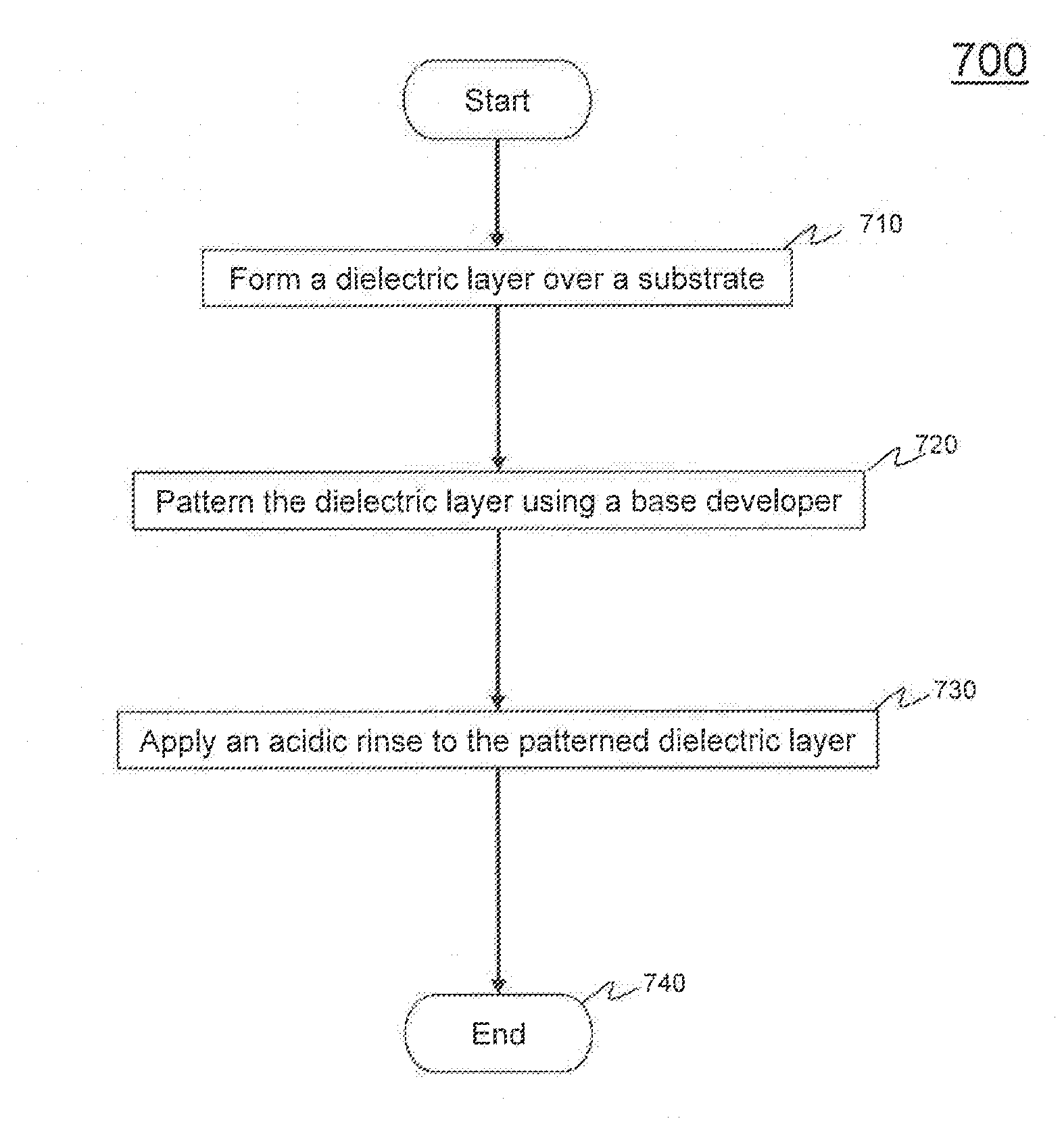
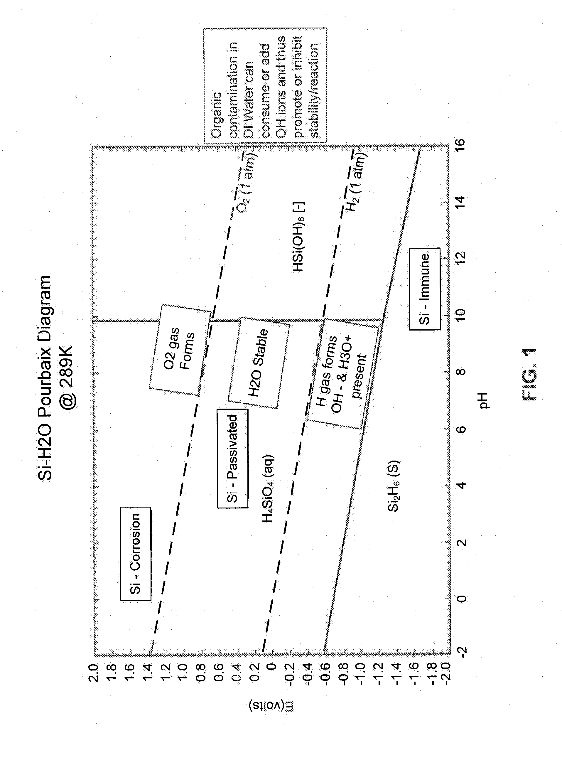
An approach is developed to use an acidic rinse to reduce charge during the lithographic process, and thereby eliminate the crystalline damage and associated yield loss associated with the accumulated charge. The crystalline damage has been found to occur for certain thicknesses of dielectric layers, and such damage is irreparable. A sparge can be used to dissolve carbon dioxide in water to provide a weak acidic rinse.

Description

BACKGROUND[0001]1. Field[0002]This invention relates generally to semiconductor lithography, and more particularly to a semiconductor processing method that avoids substrate charging that can both induce damage and attract particles.[0003]2. Background Art[0004]The semiconductor market has been undergoing extensive growth over the past few decades. This trend is expected to continue for the foreseeable future since consumer products demand more and more electronic-based features. Most electronic features rely on semiconductors, with the complexity and / or density of such semiconductors continuing to increase over time. Although complexity and / or density continue to increase over time, market forces demand that the costs decrease at the same time.[0005]Crucial to the market demand of ever decreasing cost is the ability of semiconductor manufacturers to maintain high wafer yields. Maintenance of high wafer yields requires careful attention to semiconductor processes, and a thorough und...

Claims


Application Information

Patent Timeline
Patent Type & Authority Applications(United States)
IPC IPC(8): H01L21/02H01L49/02
CPCH01L21/02164H01L21/02343H01L21/02334H01L28/40H01L21/0206H01L21/31111
Inventor SUTTON, DANIEL E.FOSTER, CHRISTOPHER M.HIGGINS, SR., KELLEY KYLEKHOGLY, MOUTASIMBIERWAG, ALEXANDER J.WILCOX, DANIEL H.
Owner CYPRESS SEMICON CORP
Why Eureka
Try Eureka