Organic el display device

a display device and organic el technology, applied in the direction of solid-state devices, semiconductor devices, thermoelectric devices, etc., can solve the problems of reduced light-emitting efficiency and high defective rate of products, and achieve the effect of large light-emitting area

Active Publication Date: 2015-06-11
JAPAN DISPLAY INC
View PDF1 Cites 18 Cited by
  • Summary
  • Abstract
  • Description
  • Claims
  • Application Information

AI Technical Summary

Benefits of technology

[0008]In an organic EL display device to emit lights of plural colors by using color filters, since an organic layer including a light-emitting layer to emit light of a single color such as W (White) color can be formed on the whole surface of a display region, an evaporation mask is not required in film growth of the light-emitting layer. Accordingly, there is a merit that high definition pixels each of which has a large light-emitting area can be manufactured. However, since a transparent resin or the like is sandwiched and adhered between a TFT (Thin Film Transistor) substrate and a counter substrate on which color filters are formed, there is a distance between the TFT substrate and the counter substrate, and there is a fear that so-called color mixture occurs in which light emitted from the light-emitting layer in an oblique direction or a lateral direction is emitted through a color filter of an adjacent pixel.

Problems solved by technology

However, since a transparent resin or the like is sandwiched and adhered between a TFT (Thin Film Transistor) substrate and a counter substrate on which color filters are formed, there is a distance between the TFT substrate and the counter substrate, and there is a fear that so-called color mixture occurs in which light emitted from the light-emitting layer in an oblique direction or a lateral direction is emitted through a color filter of an adjacent pixel.
However, in this method, since the numerical aperture is reduced, and the light-emitting efficiency is reduced.
However, if the distance is reduced, it is conceivable that the light-emitting element is damaged by a foreign substance adhered between them and the defective rate of products becomes high.

Method used


Image

  • Organic el display device
  • Organic el display device
  • Organic el display device

Examples


Embodiment Construction

[0026]Hereinafter, embodiments of the invention will be described with reference to the drawings. Incidentally, in the drawings, the same or equivalent elements are denoted by the same reference numerals and the duplicate description thereof is omitted.

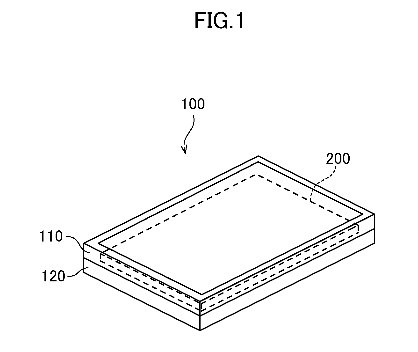
[0027]FIG. 1 schematically shows an organic EL display device 100 of an embodiment. As shown in this drawing, the organic EL display device 100 includes an organic EL panel 200 fixed so as to be sandwiched between an upper frame 110 and a lower frame 120.

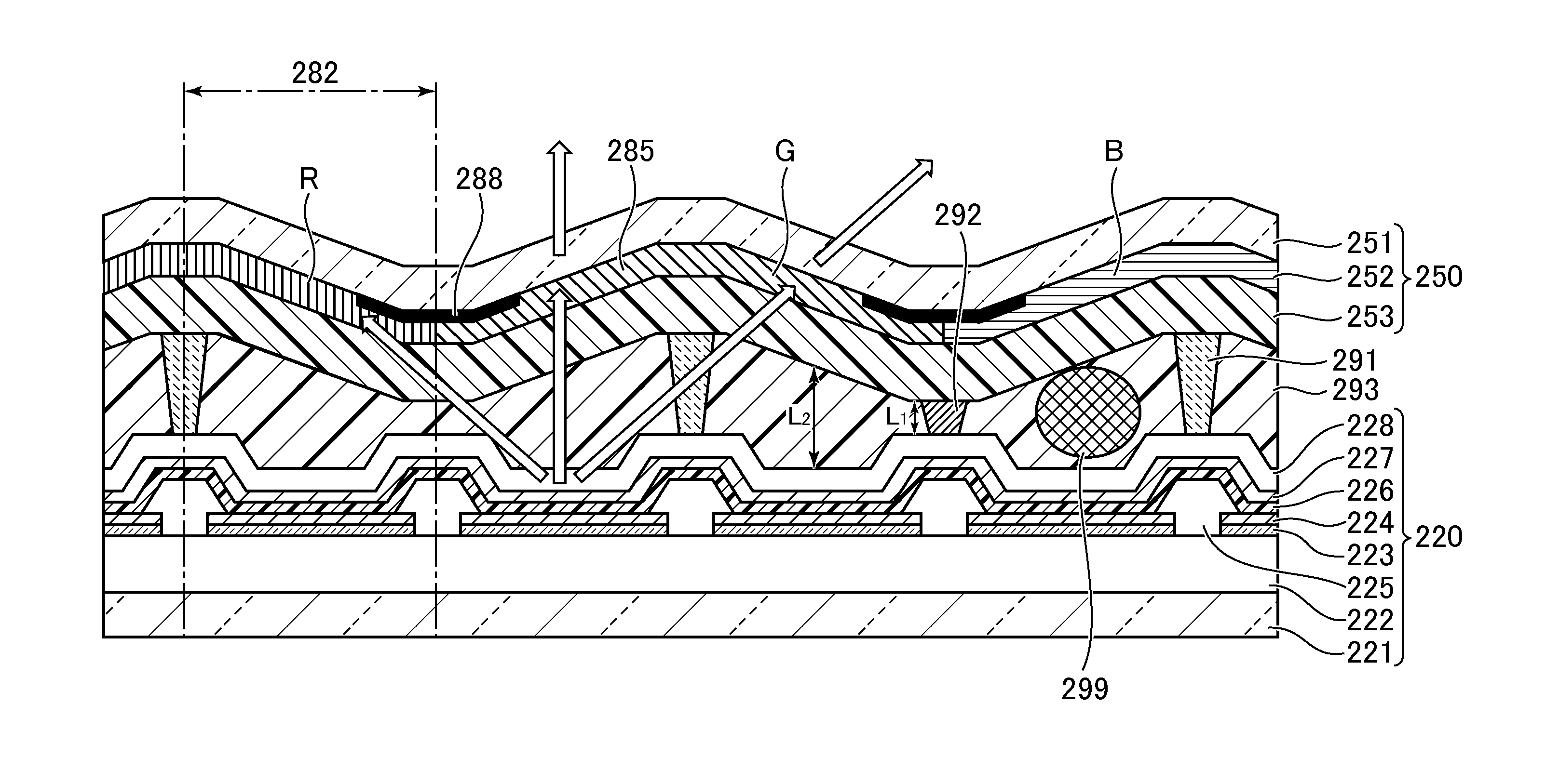
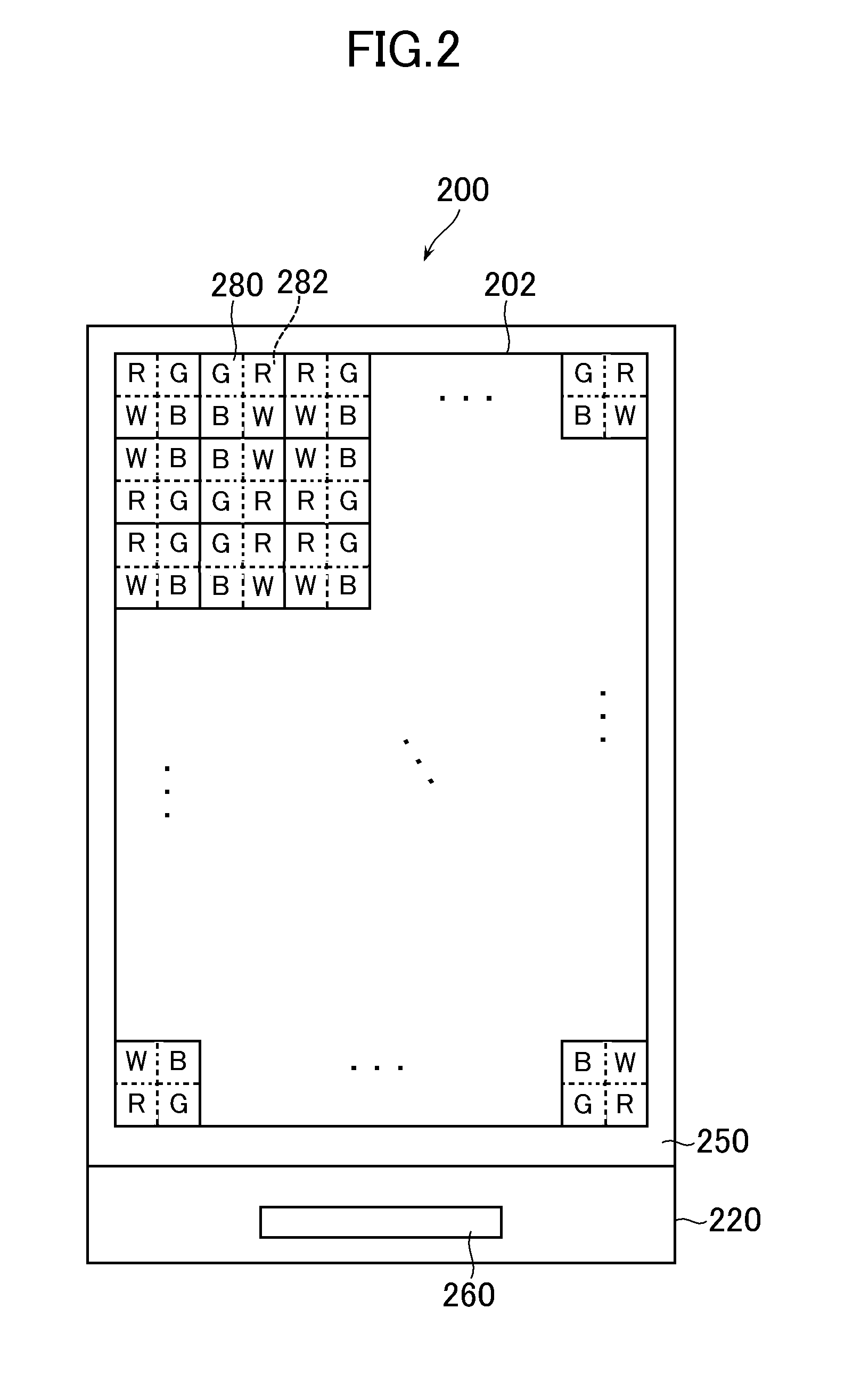
[0028]FIG. 2 shows a structure of the organic EL panel 200 of FIG. 1. The organic EL panel 200 includes two substrates of a TFT (Thin Film Transistor) substrate 220 and a counter substrate 250. A filler 293 (see FIG. 4) is filled between these substrates. The TFT substrate 220 includes pixels 280 arranged in a matrix in a display region 202. Each of the pixels 280 includes sub-pixels 282 to which four colors of R (Red), G (Green), B (Blue) and W (White) are respectively assigned. Besi...


PUM


Abstract

An organic EL display device includes a thin film transistor substrate in which a light-emitting element is provided for each of plural sub-pixels constituting each pixel, a counter substrate provided with a coupled color filter which is a color filter arranged to be extended over plural adjacent sub-pixels and allowing light in one wavelength region to pass through and a light-shielding film which is arranged on a boundary between adjacent color filters to allow lights in different wavelength regions to pass through and shields light, a filler arranged between the thin film transistor substrate and the counter substrate and made of a transparent organic material, and a filler thickness adjustment part which adjusts to cause a thickness of the filler in a region where the light-shielding film is provided to be thinner than a thickness of the filler in a region where the light-emitting element is provided.

Description

CROSS-REFERENCE TO RELATED APPLICATION[0001]The present application claims priority from Japanese application JP2013-251938 filed on Dec. 5, 2013, the content of which is hereby incorporated by reference into this application.BACKGROUND OF THE INVENTION[0002]1. Field of the Invention[0003]The present invention relates to an organic EL (Electro-Luminescent) display device.[0004]2. Description of the Related Art[0005]In recent years, an image display device (hereinafter referred to as an organic EL display device) using a self-luminous body called an organic light emitting diode is put in practical use. As compared with a related art liquid crystal display device, since the self-luminous body is used, this organic EL display device is excellent in visibility and response speed, and moreover, further thinning is possible since an assistant illumination device such as a backlight is not required.[0006]In the organic EL display device, as the organic EL display device for performing colo...

Claims


Application Information

Patent Timeline
Patent Type & Authority Applications(United States)
IPC IPC(8): H01L27/32
CPCH01L27/322H01L27/3213H01L27/3244H10K59/351H10K59/353H10K59/38H10K59/122H10K50/8428H10K50/865H10K2102/3026H10K2102/351H10K59/12
Inventor FURUIE, MASAMITSU
Owner JAPAN DISPLAY INC
Why Eureka
Try Eureka