Coaxial Impedance-Matched Test Socket

Inactive Publication Date: 2015-06-18
WOODEN TIM +1
View PDF6 Cites 34 Cited by
  • Summary
  • Abstract
  • Description
  • Claims
  • Application Information

AI Technical Summary

Benefits of technology

The tester of the invention has a unique design that allows for efficient matching of impedances between input and output. This is achieved by using a combination of a pogo pin and metal layer, with an air gap and insulation filling acting as an insulator. To further improve performance, the isolation filling between the control pogo pins and metal layers is made from a dielectric material with low dielectric permittivity. This feature is especially important for pogo pins that transmit high-frequency signals. By selecting specific dielectric materials with the required parameters, full matching can be provided.

Problems solved by technology

The increased working frequency of IC devices creates a challenge to FHST testing because traditional test sockets made out of insulative material, such as plastics and ceramics, do not perform well.
FHST test sockets made of insulative materials with high or low dielectric permittivity cannot prevent contactor crosstalk because the wavelength becomes comparable to the length of the contactors whereby the contactors behave as antennas and propagate radio frequency.
Such an approach reduces the effective number of signal connections that can be used on an IC device.
Nevertheless, all known impedance-matching devices and crosstalk-eliminating devices are relatively expensive to manufacture and are complicated in design.

Method used


Image

  • Coaxial Impedance-Matched Test Socket
  • Coaxial Impedance-Matched Test Socket
  • Coaxial Impedance-Matched Test Socket

Examples


Embodiment Construction

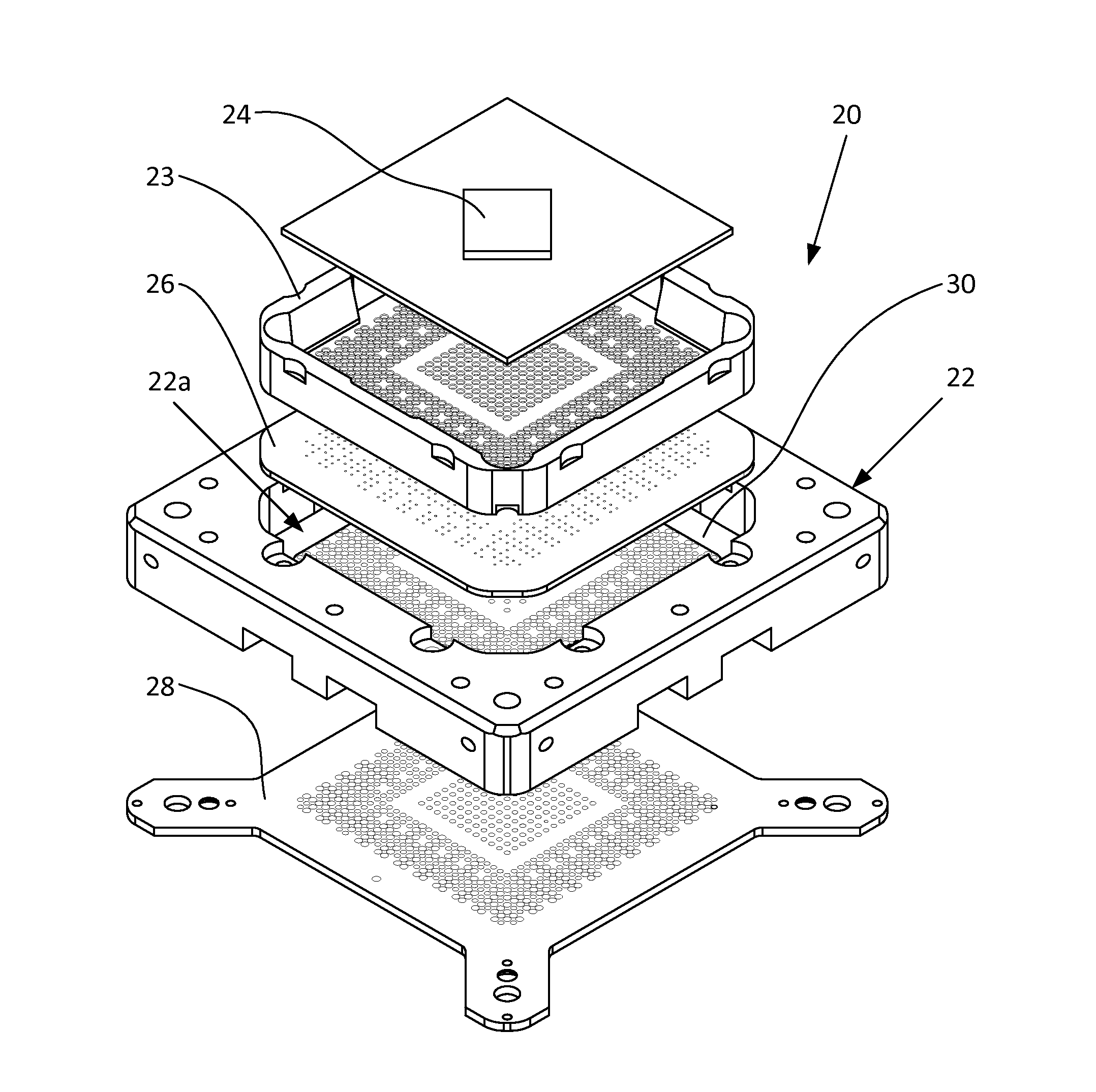
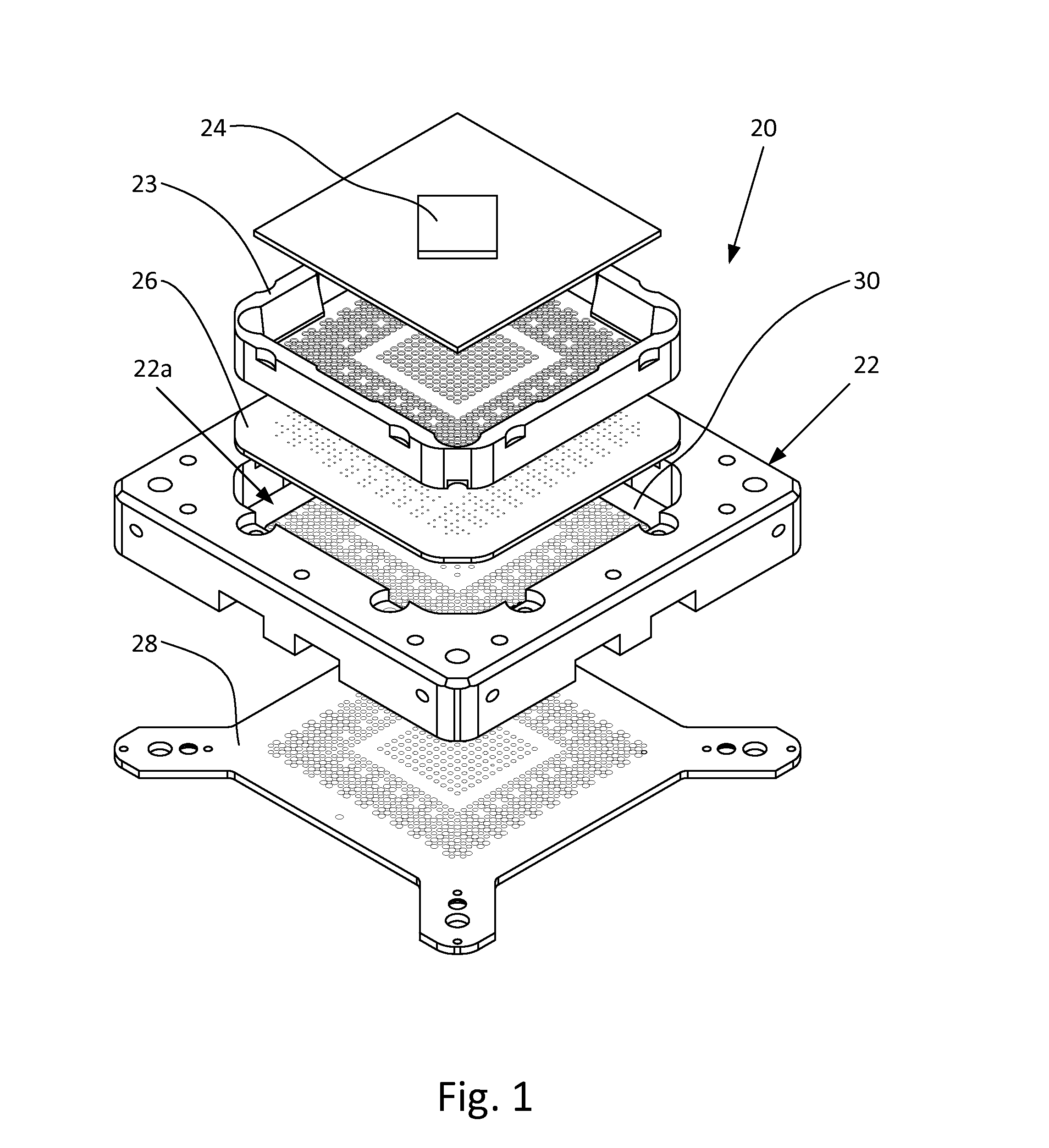
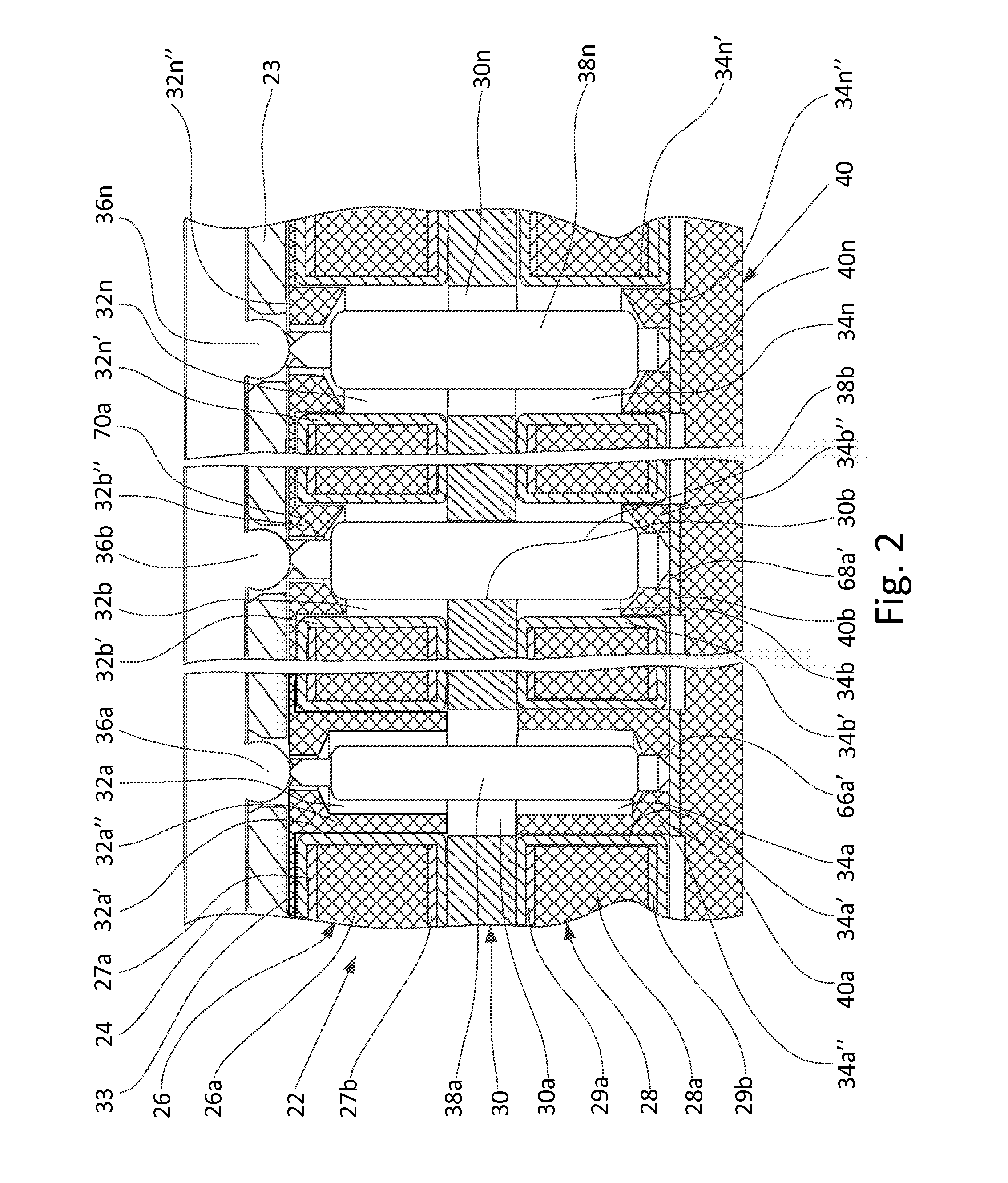
[0017]In general, when the manufacturing process of a semiconductor chip, such as an IC, or the like, is completed, the chip is tested with regard to its electrical performance, quality of electrical contacts, etc. When a semiconductor device is to be tested, a test socket is placed between the lead contacts of the integrated circuit and the terminals of the measurement device. Current flows from the test terminals of the test device (printed circuit board) into the lead terminals of the semiconductor chip through the test socket, and signals from the lead terminals are analyzed to determine IC performance and semiconductor chip abnormality.

[0018]The problem associated with the through-hole fixture arrangement is the possible bending of or damage to the test pins extending up and through the load board, thus negatively affecting the test results. To avoid this problem, a receptacle can be positioned between the fixture and the load board to protect the test pins extending through th...


PUM

PropertyMeasurementUnit
Thicknessaaaaaaaaaa
Dielectric polarization enthalpyaaaaaaaaaa
Poweraaaaaaaaaa

Abstract

A coaxial impedance-matched test socket having a socket body with a structure similar to a system of redistributed coaxial cable inserts, where the core of each insert comprises a pogo pin, a metal layer that surrounds the pogo pin functions as a shielding element of the core, and an air gap and an insulation filling between the pogo pin and the shielding metal part function as an isolator. For higher system efficiency in matching impedances between the pogo pins and the test object, the insulation fillings, which are placed between the outer surfaces of the control pogo pins and the inner surfaces of the metal layers, are made from a dielectric material of low dielectric permittivity. By selecting specific dielectric materials with the required dielectric parameters, full matching can be provided.

Description

FIELD OF THE INVENTION[0001]The present invention relates to devices for testing electrical and electronic devices with external lead contacts, such as the bumps on integrated circuit (IC) chips, in particular, to final high-speed test (FHST) sockets. More specifically, the invention provides an FHST socket that eliminates crosstalk, creates impedance-controlled signals of different values on the same socket, and at the same manufactures the mentioned sockets less expensively than traditional CNC (computer numerical control) machining by using printed circuit board technology.BACKGROUND OF THE INVENTION[0002]In general, when the process of manufacturing a semiconductor chip, such as an IC, or the like, is completed, electrical performance, quality, etc., of the semiconductor chip are tested. When a semiconductor device is to be tested, a test socket is placed between the lead contacts of the IC and the terminals of the measurement device.[0003]Current flows from the test terminals o...

Claims


Application Information

Patent Timeline
IPC IPC(8): G01R1/04G01R31/28
CPCG01R1/0466G01R31/2884G01R31/2886G01R1/07371Y10T29/49208G01R1/0441G01R3/00
Inventor WOODEN, TIMIVANKOV, SERGEY
Owner WOODEN TIM
Why Eureka
Try Eureka