Fabrication methods for back contact solar cells

a solar cell and back contact technology, applied in semiconductor/solid-state device manufacturing, electrical equipment, semiconductor devices, etc., can solve the problems of reducing production yield, affecting the efficiency of back contact solar cells, so as to reduce or eliminate disadvantages and problems.

Inactive Publication Date: 2015-06-18
BEAMREACH SOLAR INC
View PDF5 Cites 44 Cited by
  • Summary
  • Abstract
  • Description
  • Claims
  • Application Information

AI Technical Summary

Benefits of technology

[0009]Therefore, a need has arisen for fabrication methods for back contact solar cells. In accordance with the disclosed subject matter, methods for the fabrication of back contact solar cells are provided. These innovations substantially reduce or eliminate disadvantages and problems associated with previously developed back contact solar cell fabrication methods.

Problems solved by technology

Although moving to thinner crystalline silicon solar cells is long understood to be one of the most potent and effective methods for PV cost reduction (because of the relatively high material cost of crystalline silicon wafers used in solar cells as a fraction of the total PV module cost), utilizing thinner crystalline wafers is hampered by the problem of thin wafers being extremely fragile, mechanical breakage during wafer handling and cell processing, and the resulting production yield losses caused by thin and fragile silicon wafers.
Other problems include inadequate light trapping in the thin cell structure because silicon is an indirect bandgap semiconductor material and absorption of longer wavelength red and infrared photons (particularly those in the wavelength range of about 900 nm to 1150 nm) requires relatively long optical path lengths—often much larger than the wafer thickness itself.
Further, using known designs and manufacturing technologies it is often difficult to balance the requirement of high mechanical yield and reduced wafer breakage rate with high manufacturing yields in PV factories in a cost effective manner.
Relating to substrate (semiconductor absorber) thickness, for current crystalline silicon wafer solar cells, moving even slightly thinner than the current thickness range of 140 μm to 200 μm starts to severely compromise mechanical yield during cell and module manufacturing.
This is particularly a big challenge for larger cell sizes such as 156 mm×156 mm and 210 mm×210 mm cells (compared to the smaller 125 mm×125 mm cells).
In the past, there have been attempts in solar PV R&D to use carriers such as glass for thin substrates; however, these carriers have suffered from serious limitations including relatively low maximum processing temperatures in the case of soda lime glass (or most other non-silicon foreign materials), with the processing temperatures being limited to well below approximately 400° C.—which potentially may compromise the solar cell efficiency.

Method used


Image

  • Fabrication methods for back contact solar cells
  • Fabrication methods for back contact solar cells
  • Fabrication methods for back contact solar cells

Examples


second embodiment

[0078]a permanent “Backplanes without Metallization” is a design known as acronym “PLUTO.” In this process flow, a simple and cheap backplane material (e.g., a relatively low-CTE Pre-preg material comprising a mixture of resin and fibers) is attached to the TFSS, while it is attached to the first carrier. The backplane attachment may be a direct bonding / lamination (if material has adhesive in it) or use an intermediate adhesive layer, for example a dielectric adhesive (DA) which may be printed using means such as screen printing (or applied using a spray coater or a roller coater). The pre-preg assembly / material choices should be such that they meet the following criteria:[0079]a. The released TFSS / Pre-preg assembly should be relatively stress and crack-free with very little bow.[0080]b. The backplane should maintain crack-free properties and should not induce stress cracks in the TFSS, while going through subsequent processing steps such as frontside texturing (e.g., using hot KOH)...

third embodiment

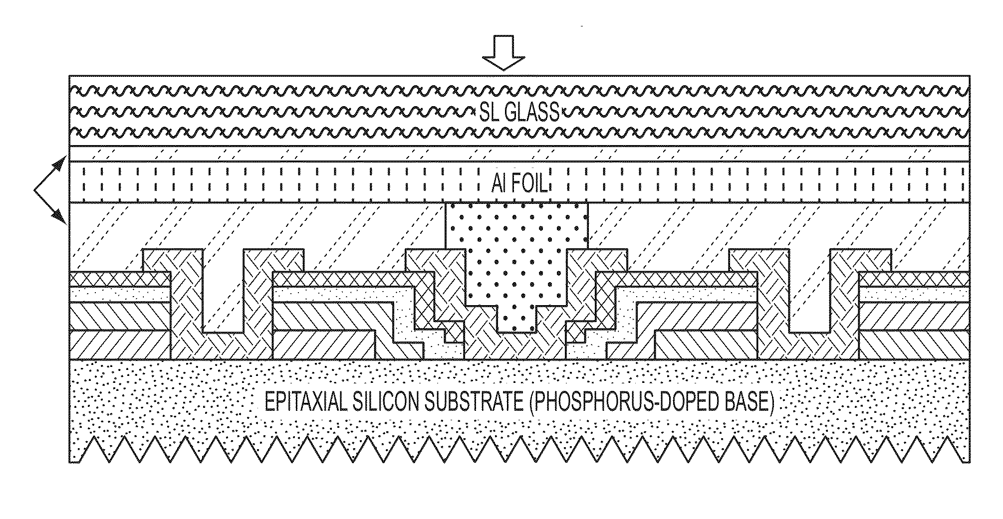
[0082]The third embodiment, “Cu Plugs,” of a permanent “Backplanes without Metallization” of FIG. 1 is a design with a slight modification of the aforementioned so-called PLUTO embodiment. And although, specifically identified with a metal as a naming convention, this approach should not be construed to be limited to copper as the electrically conductive material. In this case, the backplane has an additional layer backing compared to PLUTO. For example, the backplane may consists of glass or other harder solid backsheet materials (e.g., anodized Al) with a pliant attachment material such as an encapsulant PV-FS Z68 (from DNP Solar), also called Z68 in short, or Ethylene Vinyl Acetate (EVA). The backsheet may have pre-drilled holes, but the underlying attachment material serves as a sealant to protect the TFSS metal from being chemically attacked during frontside processing (such as during frontside wet alkaline texturing). After texture and passivation processes, the sealant materi...

first embodiment

[0153]FIG. 19, a hot ablation direct writing process, depicts a minimum steps process flow with the following noted attributes: two APCVD process steps used, has a texturing process, uses PSG and hot ablation to form base diffusion, selective emitter formed using laser, has a direct metal write process such as screen print, inkjet, aerosol print, laser transfer print, and direct solder bonding without CE screen print.

[0154]FIG. 20, a cold ablation direct writing process, depicts a second embodiment of the minimum process flow. It retains the common attributes of FIG. 19 of solder attachment as well as direct metal write to eliminate a few process steps. However, it differs from the FIG. 19 flow in that it does not rely on hot ablation and has three APCVD steps.

[0155]Non Epi Bulk Thin Substrate Process Flows.

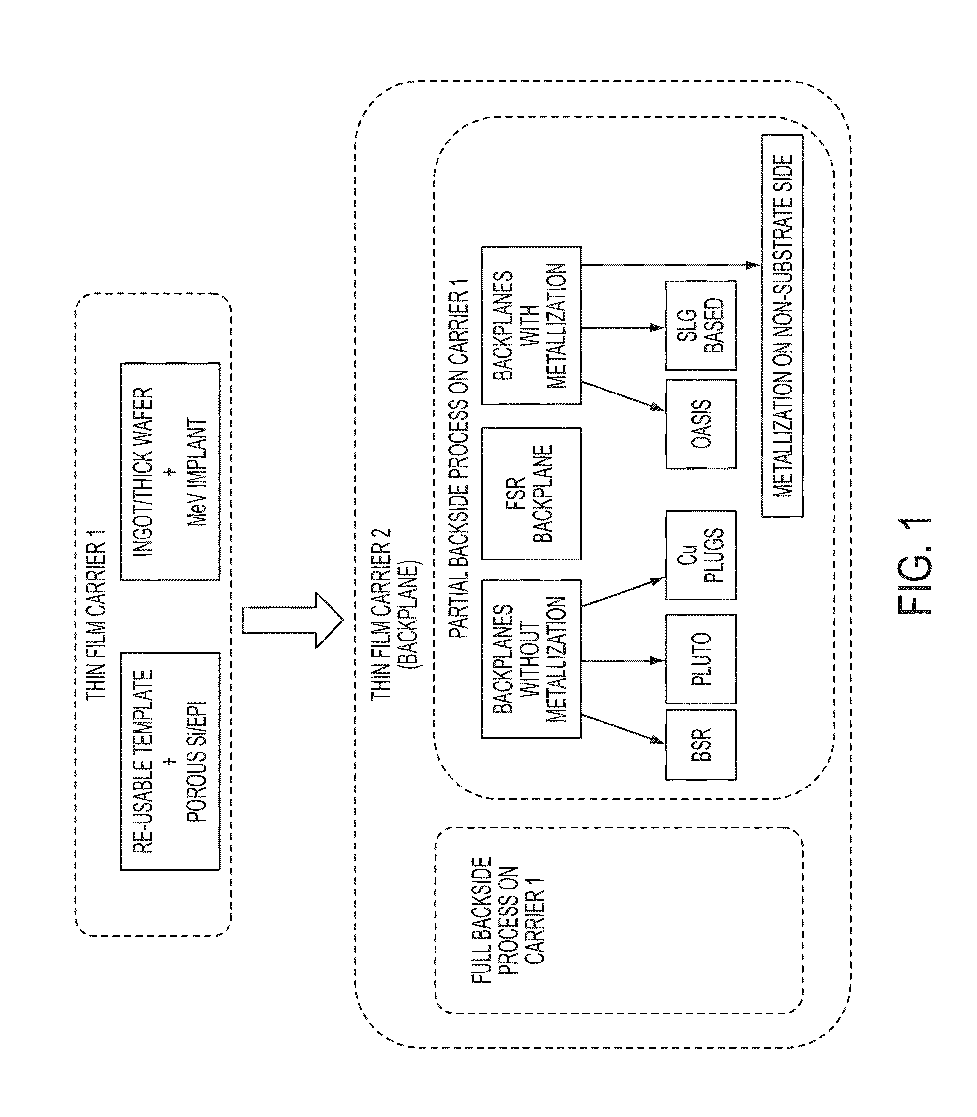
[0156]Previously, two types of carrier 1 examples were disclosed. The first type of carrier 1 uses a template and the second type of carrier 1 is a thicker wafer or ingot from wh...


PUM


Abstract

Fabrication methods for forming thin film back contact solar cells are provided.

Description

CROSS-REFERENCE TO RELATED APPLICATIONS[0001]This application claims priority to U.S. Provisional Pat. App. No. 61 / 880,777 filed Sep. 20, 2013 which is hereby incorporated by reference in its entirety.[0002]This application is a continuation in part of U.S. patent Ser. No. 13 / 731,112 filed Dec. 31, 2012 which claims priority to U.S. Provisional Pat. App. No. 61 / 582,184, filed Dec. 30, 2011, which are both hereby incorporated by reference in their entirety.[0003]U.S. patent Ser. No. 13 / 731,112 is also a continuation in part of U.S. patent Ser. No. 13 / 807,631 filed Dec. 28, 2012, and which claims priority to P.C.T. Pat. No. PCT / US12 / 00348 filed Aug. 9, 2012, and which claims priority to U.S. Provisional Pat. App. Nos. 61 / 521,754 and 61 / 521,743 both filed Aug. 9, 2011, which are all hereby incorporated by reference in their entirety.FIELD[0004]The present disclosure relates in general to the fields of photovoltaics and semiconductor microelectronics. More particularly, the present disc...

Claims


Application Information

Patent Timeline
Patent Type & Authority Applications(United States)
IPC IPC(8): H01L31/02H01L31/18H01L31/0224H01L31/0216
CPCH01L31/02008H01L31/022441H01L31/1864H01L31/02168H01L31/0516H01L31/056H01L31/0682H01L31/1892Y02E10/52Y02E10/547
Inventor KAPUR, PAWANDESHPANDE, ANANDRANA, VIRENDRA V.MOSLEHI, MEHRDAD M.SEUTTER, SEAN M.
Owner BEAMREACH SOLAR INC
Why Eureka
Try Eureka