Display panel and method of manufacturing the same

a technology of display panel and sealing member, which is applied in the field of display panel, can solve the problems of cathode ray tube display device, high power consumption, thick thickness, etc., and achieve the effects of improving the adhesion strength of the sealing member used to couple the substrate, improving the visibility of the display panel, and low reflection characteristics

Active Publication Date: 2015-07-02
SAMSUNG DISPLAY CO LTD
View PDF3 Cites 31 Cited by
  • Summary
  • Abstract
  • Description
  • Claims
  • Application Information

AI Technical Summary

Benefits of technology

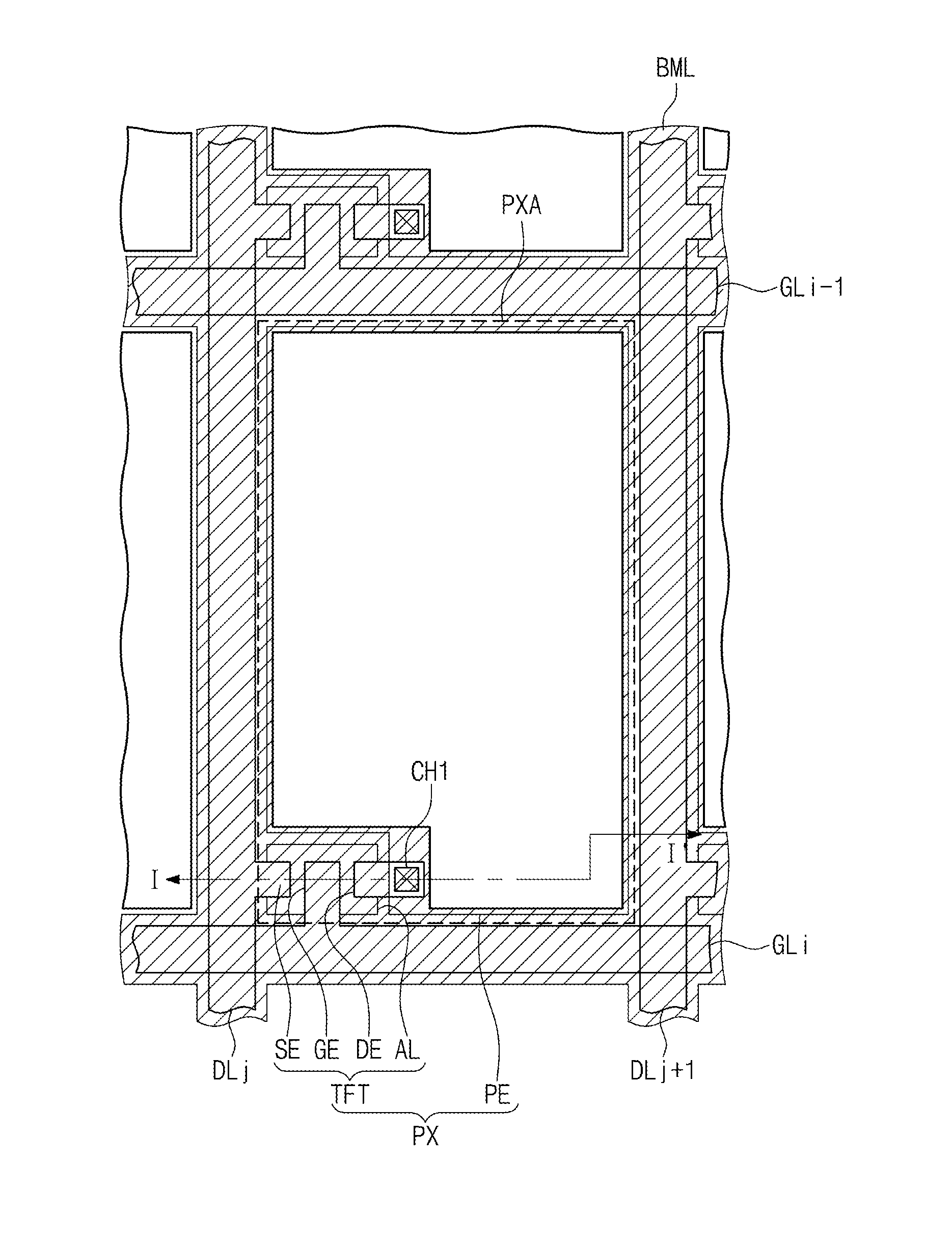
[0031]According to the above, since the color filter layer and the black matrix layer are disposed on an array substrate and the black matrix layer is not disposed on an opposite substrate facing the array substrate, an organic layer required to planarize the black matrix layer may be omitted. Accordingly, the common electrode disposed on the opposite substrate is adhered to the upper surface of the substrate and the adhesive strength of the sealing member used to couple the substrates is improved, and thus moisture may be prevented from penetrating in to an interface between the sealing member and the common electrode or between the common electrode and the substrate.
[0032]In addition, the black matrix layer is buried in the base substrate and the elements of the array substrate, but has the low reflection characteristic. Therefore, the visibility of the display panel may be improved even though the black matrix layer including the metal material is used.

Problems solved by technology

A flat panel display device has been developed to replace a cathode ray tube display device with thick thickness and high power consumption.

Method used


Image

  • Display panel and method of manufacturing the same
  • Display panel and method of manufacturing the same
  • Display panel and method of manufacturing the same

Examples


Embodiment Construction

[0044]It will be understood that when an element or layer is referred to as being “on”, “connected to” or “coupled to” another element or layer, it can either be formed directly on, connected or coupled to the other element or layer, or formed with intervening elements or layers. In contrast, when an element is referred to as being “directly on,”“directly connected to” or “directly coupled to” another element or layer, there are no intervening elements or layers present. Like numbers refer to like elements throughout. As used herein, the term “and / or” includes any and all combinations of one or more of the associated listed items.

[0045]It will be understood that, although the terms first, second, etc. may be used herein to describe various elements, components, regions, layers and / or sections, the described elements, components, regions, layers and / or sections are not limited by the terms used. The terms are only used to distinguish one element, component, region, layer or section f...


PUM

PropertyMeasurementUnit
reflectivityaaaaaaaaaa

Abstract

A display panel includes a first base substrate that includes an upper surface to which an external light is incident and a lower surface facing the upper surface and includes a plurality of pixel areas and a peripheral area adjacent to the pixel areas when viewed in a plan view, a plurality of pixels disposed on the lower surface of the first base substrate to respectively correspond to the pixel areas, and a black matrix layer disposed between the pixels and the lower surface of the first base substrate to overlap the peripheral area. The black matrix layer includes a low reflection layer disposed on the lower surface of the first base substrate and a light blocking layer disposed on the low reflection layer.

Description

CROSS-REFERENCE TO RELATED APPLICATION[0001]This U.S. non-provisional patent application claims priority under 35 U.S.C. §119 of Korean Patent Application No. 10-2013-0165578, filed on Dec. 27, 2013, the contents of which are hereby incorporated by reference in its entirety.BACKGROUND[0002]1. Field of Disclosure[0003]The present disclosure relates to a display panel and a method of manufacturing the same. More particularly, the present disclosure relates to a display panel including a low reflection black matrix and a method of manufacturing the display panel.[0004]2. Description of the Related Art[0005]A flat panel display device has been developed to replace a cathode ray tube display device with thick thickness and high power consumption. As the flat panel display device, various display devices, such as an organic light emitting display device, a liquid crystal display device, a plasma display panel device, etc., are widely used.[0006]Each display device includes pixels and sign...

Claims


Application Information

Patent Timeline
Patent Type & Authority Applications(United States)
IPC IPC(8): H01L27/12G02F1/1368G02F1/1362H01L29/786
CPCH01L27/124H01L27/1259G02F1/136209G02F1/1368H01L29/7869G02F2203/09H01L27/1218H01L27/1225H01L29/78633G09F9/30
Inventor PARK, EUN-KILKANG, HYUN-HO
Owner SAMSUNG DISPLAY CO LTD
Why Eureka
Try Eureka