Organic light emitting display device and manufacturing method thereof

a technology of light-emitting display device and manufacturing method, which is applied in the direction of organic semiconductor device, thermoelectric device, solid-state device, etc., can solve the problems of gate electrode b>11/b> damage, and loss of contact hole ck, etc., to reduce the number of mask procedures and enhance the reliability of elements

Active Publication Date: 2015-07-02
LG DISPLAY CO LTD
View PDF3 Cites 14 Cited by
  • Summary
  • Abstract
  • Description
  • Claims
  • Application Information

AI Technical Summary

Benefits of technology

[0022]The embodiments provide an organic light emitting display device and a manufacturing method thereof which are adapted to prevent damage of a gate electrode, a storage electrode and pads by forming a barrier layer of a conductive oxide semiconductor material on a gate metal film.
[0023]The embodiments provide an organic light emitting display device and a manufacturing method thereof which are adapted to enhance reliability of elements and reduce the number of mask procedures by forming a barrier layer of a conductive oxide semiconductor material on a gate electrode, a storage electrode and pads.

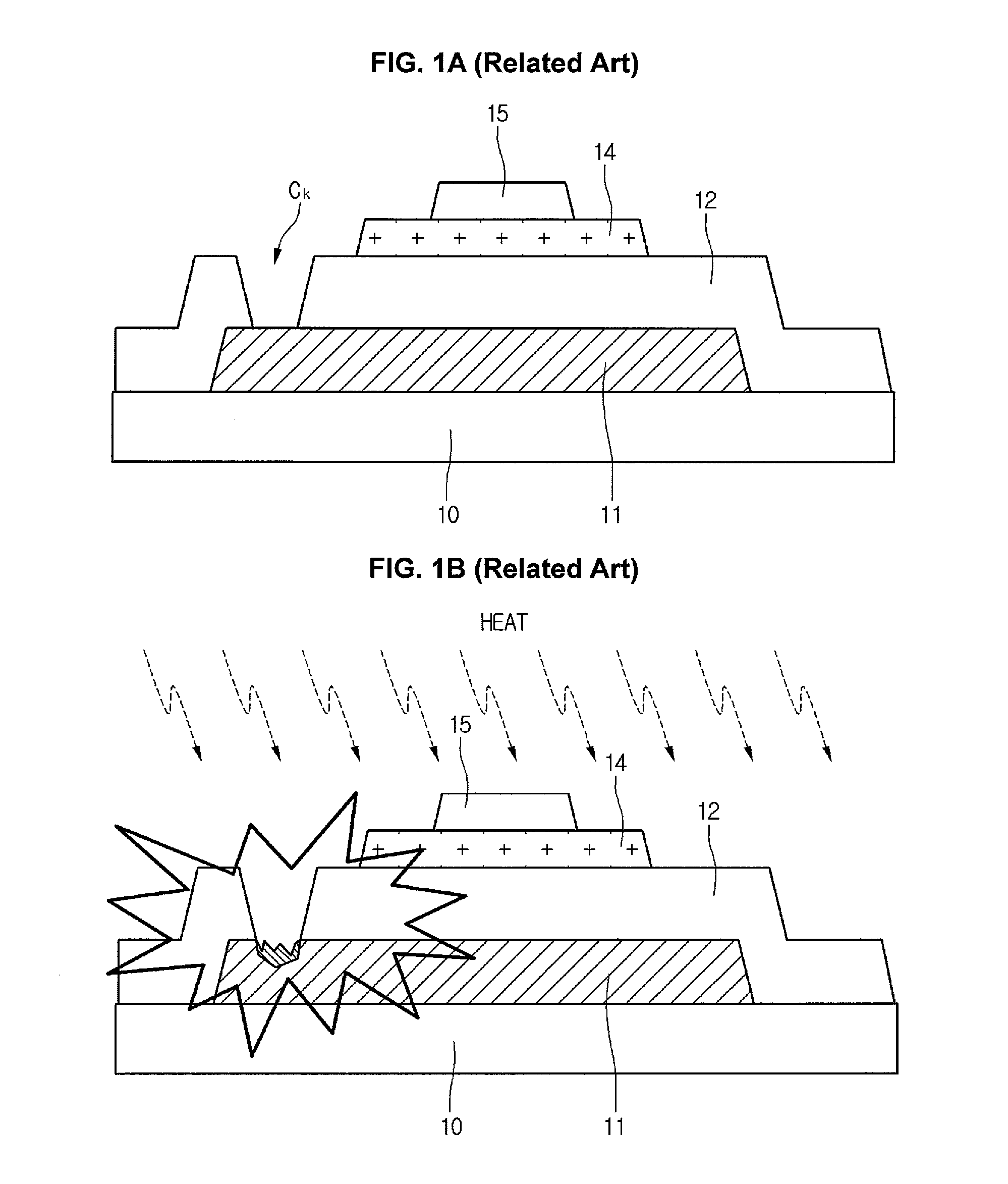
Problems solved by technology

However, a part of the gate electrode 11 exposed the contact hole Ck can be damaged due to the heat treatment process.
Due to this, the gate electrode 11 might be damaged during the etching process and the heat treatment process.
As such, the storage electrode and the gate and data pads can be damaged during the formation procedure of the etch stopper 15.
These damages result in reliability deterioration of the elements and quality deterioration of images.

Method used


Image

  • Organic light emitting display device and manufacturing method thereof
  • Organic light emitting display device and manufacturing method thereof
  • Organic light emitting display device and manufacturing method thereof

Examples


Embodiment Construction

[0034]Reference will now be made in detail to embodiments of the present invention, examples of which are illustrated in the accompanying drawings. These embodiments introduced hereinafter are provided as examples in order to convey their spirits to the ordinary skilled person in the art. Therefore, these embodiments might be embodied in a different manner, so that they are not limited to these embodiments described here. Also, the size and thickness of the device might be exaggerated for the sake of convenience in the drawings. Wherever possible, the same reference numbers will be used throughout this disclosure including the drawings to refer to the same or like parts.

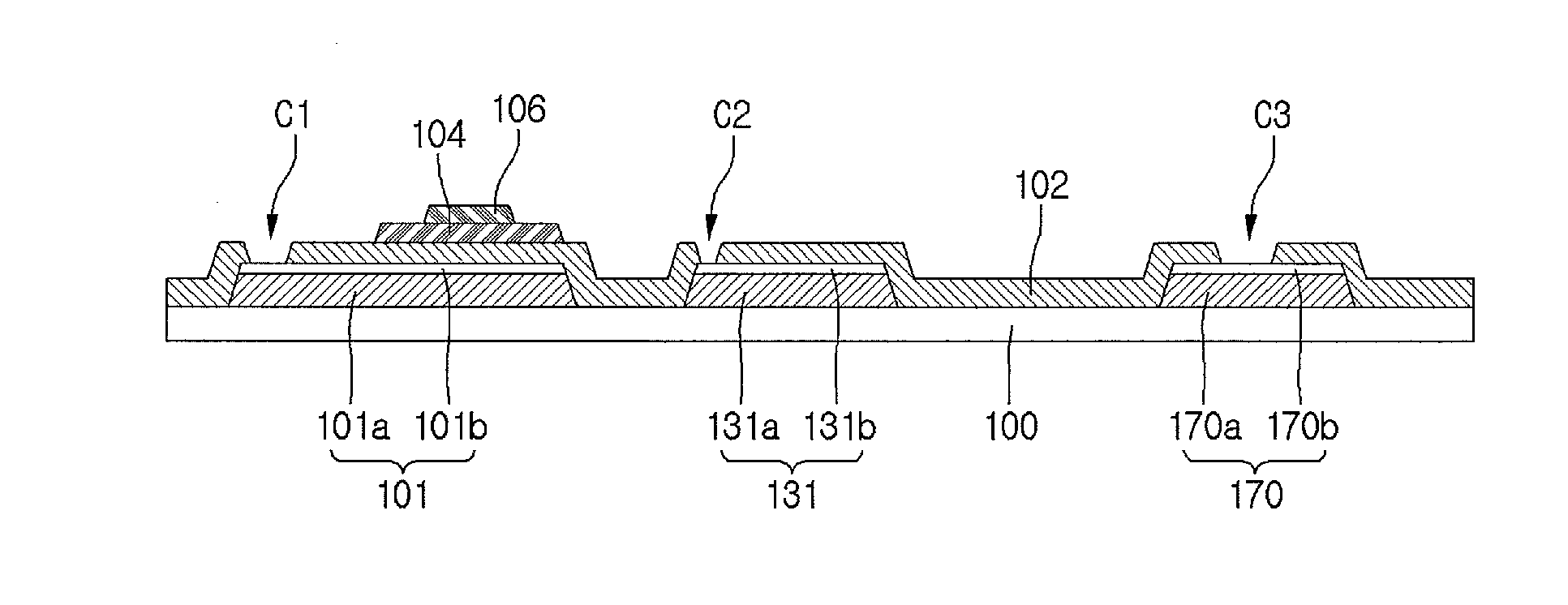
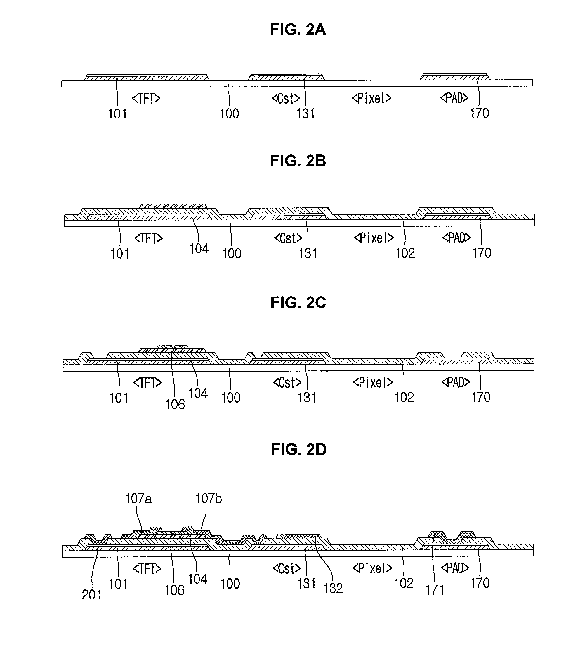
[0035]FIGS. 2A through 2K are cross-sectional views illustrating an OLED manufacture method according to an embodiment of the present invention.

[0036]Referring to FIGS. 2A through 2K, the OLED device manufacture method according to an embodiment of the invention forms a gate electrode 101 on a substrate 100. The subs...


PUM

PropertyMeasurementUnit
threshold voltageaaaaaaaaaa
conductiveaaaaaaaaaa

Abstract

A method of fabricating an organic light emitting display device is discussed. The method in one example includes: sequentially forming a first metal film and a second metal film on a substrate and performing a mask procedure for the first and second metal films, to form a gate electrode, a first storage electrode and a pad in a thin film transistor region, a storage capacitor region and a pad region; forming a gate insulation film on the substrate provided with the gate electrode; forming a third storage electrode which overlaps the second storage electrode with a passivation film therebetween and is connected to the drain electrode; forming red, green and blue color filters in respective pixel regions of the substrate; and forming an organic light emitting diode on the substrate provided with the color filter.

Description

CROSS REFERENCES TO RELATED APPLICATIONS[0001]The present application claims priority under 35 U.S.C. §119(a) to Korean Patent Application No. 10-2013-0167693 filed in the Republic of Korea on Dec. 30, 2013, which is hereby incorporated by reference in its entirety.BACKGROUND OF THE INVENTION[0002]1. Field of the Disclosure[0003]The present application relates to an organic light emitting display device. More particularly, the present application relates to an organic light emitting display device adapted to enhance reliability of elements and reduce the number of mask procedures, and to a method of manufacturing the same.[0004]2. Description of the Related Art[0005]Recently, flat panel display devices are being developed for replacing cathode ray tube devices (CRTs), which are heavy and have large volume. The flat panel display devices include liquid crystal display (LCD) devices and organic light emitting display (OLED) devices.[0006]OLED devices are self-luminous and do not need ...

Claims


Application Information

Patent Timeline
Patent Type & Authority Applications(United States)
IPC IPC(8): H01L51/52H01L51/56H01L27/32
CPCH01L51/5253H01L27/322H01L27/3265H01L2251/303H01L51/56H01L51/5221H01L27/3262H01L27/124H01L27/1255H10K59/126H10K50/82H10K59/00H10K59/131H10K50/125H10K59/38H10K59/124H10K71/00H10K59/1201H01L27/1225H01L29/4958
Inventor JANG, YI SIK
Owner LG DISPLAY CO LTD
Why Eureka
Try Eureka