MEMS device and method of manufacturing

a technology of microelectromechanical systems and manufacturing methods, applied in the field of microelectromechanical systems (mems) devices, can solve the problems of high device cost, up to 50-80% of the final packaging device's cost, and much effort in developing packaging methods, and achieve the effect of cost-effectiveness

Active Publication Date: 2015-07-09
MOTION ENGINE
View PDF3 Cites 22 Cited by
  • Summary
  • Abstract
  • Description
  • Claims
  • Application Information

AI Technical Summary

Benefits of technology

[0008]What is needed is a MEMS device which allows transmitting electrical signals from within the device to at least one cap, while

Problems solved by technology

Consequently, much effort has gone into developing methods of packaging MEMS devices to protect them while providing access to electrical signals.
This labor intensive and materially demanding chip-level packaging may account for up to 50-80% of the final packaged

Method used


Image

  • MEMS device and method of manufacturing
  • MEMS device and method of manufacturing
  • MEMS device and method of manufacturing

Examples


Embodiment Construction

[0055]Within the following description, similar features of the drawings have been given similar reference numerals. To preserve the clarity of the drawings, some reference numerals have been omitted when they were already identified in a preceding figure.

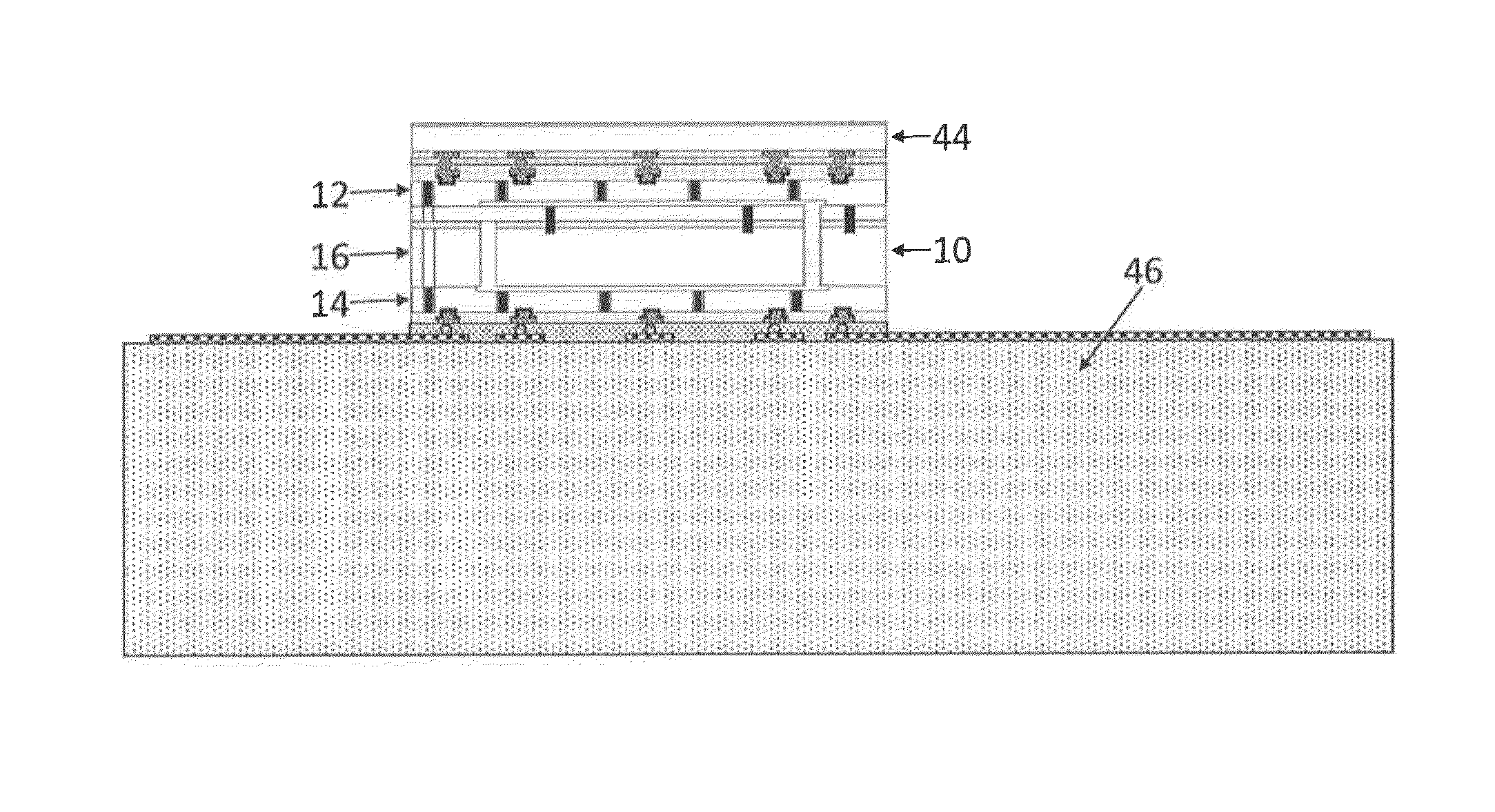
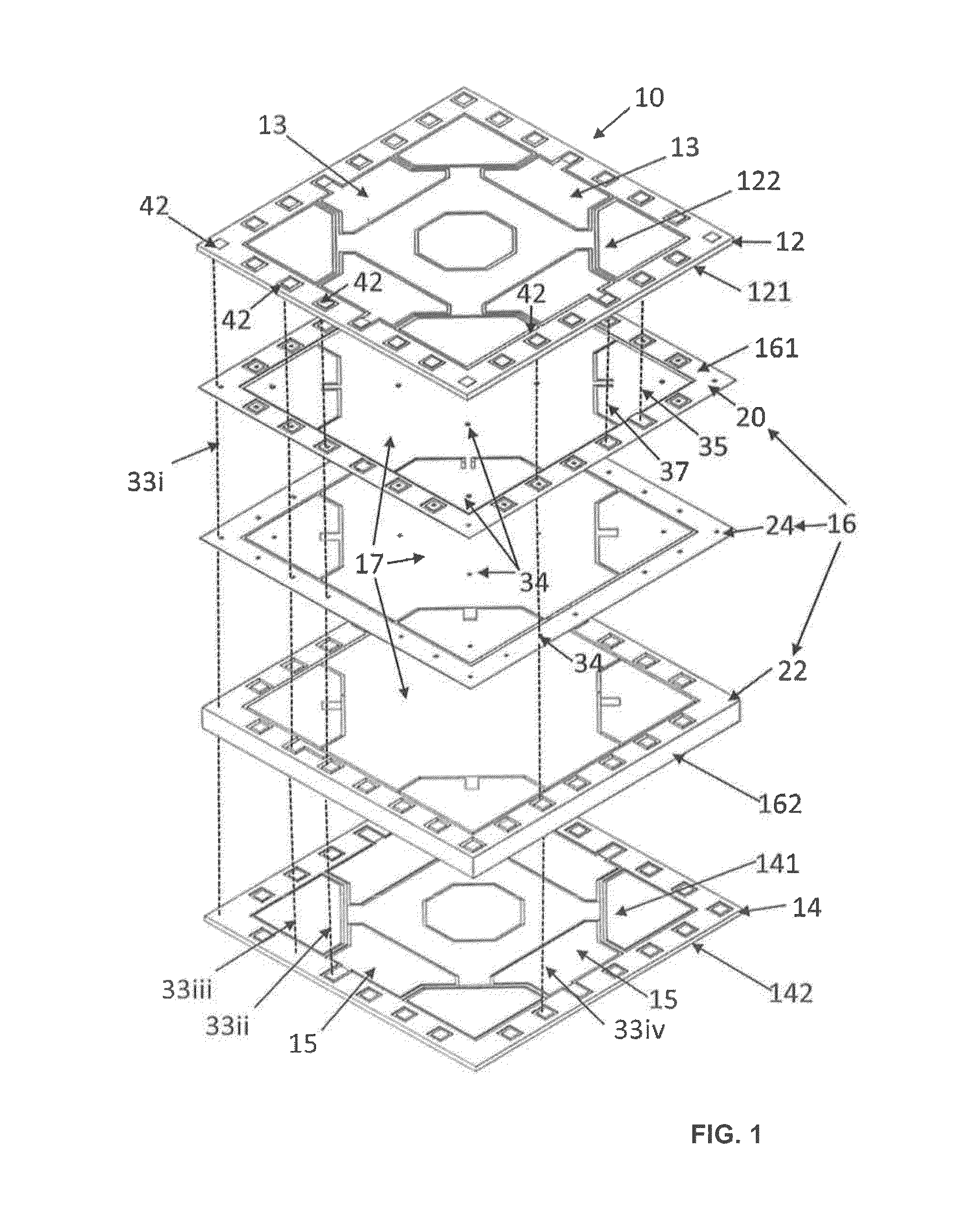
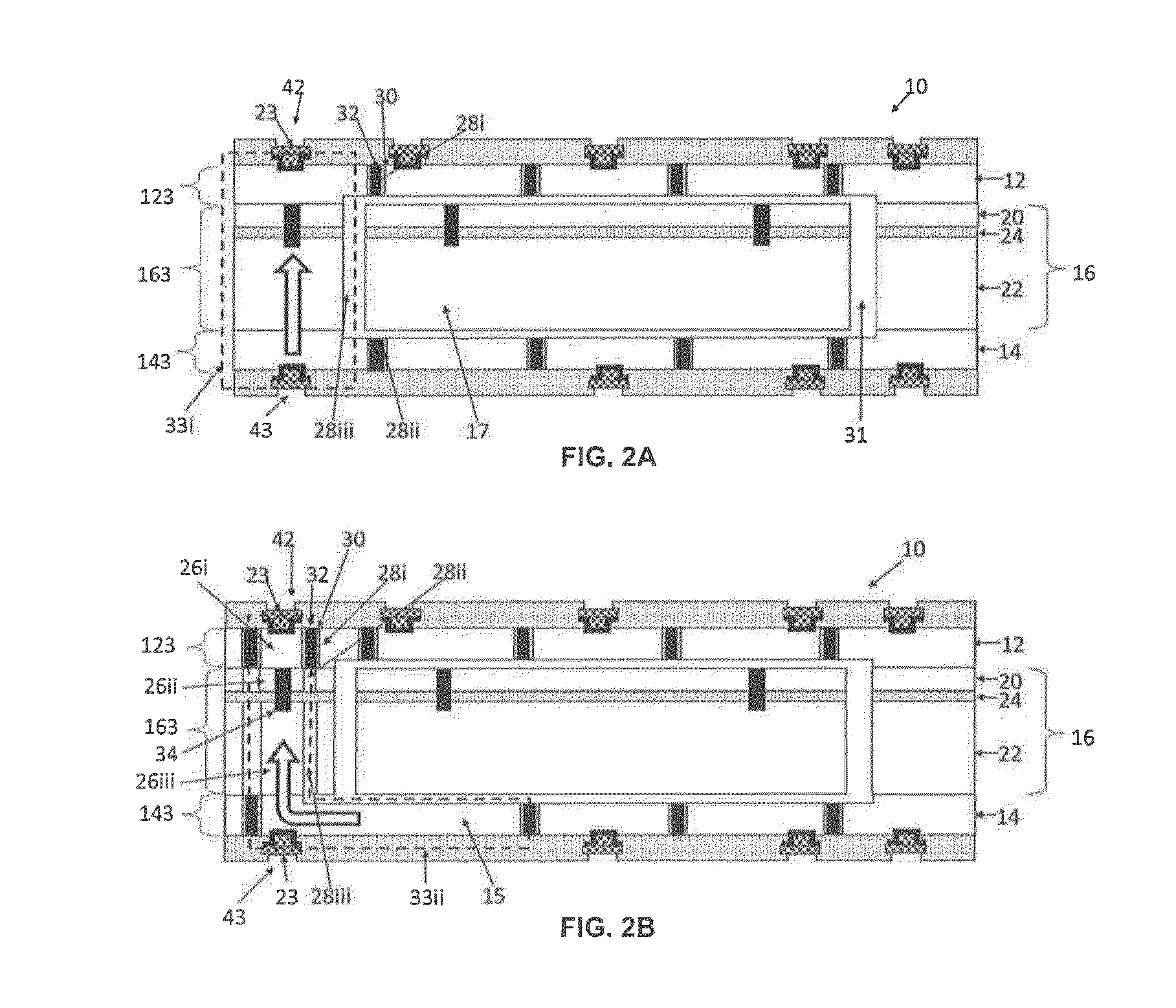
[0056]The present invention provides a MEMS device formed by a top cap wafer, a central MEMS wafer and a bottom cap wafer, the wafers being made of an electrically conducting material, such as silicon. The MEMS device includes insulated conducting pathways extending from the bottom cap wafers, through the MEMS wafer and to the top cap wafers, allowing routing or transmitting electrical signals through the MEMS device, from the bottom cap wafer to the top cap wafer. This architecture of the MEMS device enables the placement of electrodes and electrical leads above, below, and / or around MEMS structure(s)—such as membrane(s) or diaphragm(s), proof masse(s)micro-valve(s), sensor(s) and transducer(s), comb sensor(s), micro-pumps, etc., ...


PUM

PropertyMeasurementUnit
Thicknessaaaaaaaaaa
Electrical conductivityaaaaaaaaaa
Electrical conductoraaaaaaaaaa

Abstract

A MEMS device is provided. The device includes a MEMS wafer, a top cap wafer and a bottom cap wafer. The top and bottom cap wafers are respectively bonded to first and second sides of the MEMS wafer, the MEMS and cap wafers being electrically conductive. The outer side of the top cap wafer is provided with electrical contacts. The MEMS wafer, the top cap wafer and the bottom cap wafer define a cavity for housing a MEMS structure. The device includes insulated conducting pathways extending from within the bottom cap wafer, through the MEMS wafer and through the top cap wafer. The pathways are connected to the respective electrical contacts on the top cap wafer, for routing electrical signals from the bottom cap wafer to the electrical contacts on the top cap wafer. A method of manufacturing the MEMS device is also provided.

Description

RELATED APPLICATIONS[0001]This patent application is a continuation-in-part of International Application No. PCT / CA2014 / 050635 filed on Jul. 4, 2014, which claims priority from U.S. Application No. 61 / 843,598 filed on Jul. 8, 2013, the disclosure of these applications being incorporated herein by reference in their entirety.TECHNICAL FIELD OF THE INVENTION[0002]This invention relates to MicroElectroMechanical Systems (MEMS) devices enabling electrical measurements from top and / or bottom caps. The invention also relates to a method of manufacturing MEMS devices.BACKGROUND[0003]MicroElectroMechanical Systems, or MEMS, are an enabling technology. Generally speaking, MEMS devices are integrated circuits containing tiny mechanical, optical, magnetic, electrical, chemical, biological, or other, transducers or actuators. They are manufactured using high-volume silicon wafer fabrication techniques developed over the last 50 years for the microelectronics industry. Their resulting small size...

Claims


Application Information

Patent Timeline
IPC IPC(8): B81B7/00B81C1/00
CPCB81C1/00301B81B7/007B81B2207/095B81B2207/096H01L2224/49171H01L2224/94
Inventor BOYSEL, ROBERT MARKROSS, LOUIS
Owner MOTION ENGINE
Why Eureka
Try Eureka