Light emitting module and lens

a technology of light-emitting modules and lenses, which is applied in the direction of instruments, lighting and heating apparatus, semiconductor devices of light sources, etc., can solve the problems of increasing power consumption, limiting the implementation of high-quality picture quality, and the difference in contrast of edge-type backlights, etc., to achieve uniform surface light sources, easy to fabricate lenses, and elongated light orientation patterns

Active Publication Date: 2015-07-09
SEOUL SEMICONDUCTOR
View PDF25 Cites 15 Cited by
  • Summary
  • Abstract
  • Description
  • Claims
  • Application Information

AI Technical Summary

Benefits of technology

[0012]Another aspect of the present invention is directed to a lens for dispersing light and a light emitting module including the same, and more particularly, to a lens and a light emitting module capable of increasing an alignment tolerance between an LED and a lens.
[0014]Another aspect of the present invention is directed to a lens and a light emitting module that are easy to fabricate.
[0018]In some embodiments, light scattering patterns may be formed on at least one of the surface perpendicular to the central axis and the downwardly convex surface within the concave portion of the lower surface and on a surface positioned closer to the central axis than the at least one surface. A light scattering pattern may be formed with an uneven pattern, and may further disperse light emitted from the light emitting diode to the vicinity of the central axis.
[0034]In some embodiments, light scattering patterns may be formed on at least one of the surface perpendicular to the central axis and the downwardly convex surface within the concave portion of the lower surface and on a surface positioned closer to the central axis than the at least one surface. A light scattering pattern may be formed with an uneven pattern, and may further disperse light emitted from the light emitting diode to the vicinity of the central axis.
[0040]According to embodiments of the present invention, since primary refraction occurs in a concave portion of a lens and secondary refraction occurs in an upper surface of the lens, the lens can extensively disperse light. In addition, since an upper end of the concave portion of the lens is shaped to include a flat surface or a convex surface, instead of a concave surface, an alignment tolerance between an LED chip or a light emitting device and the lens can be increased. Furthermore, since a change in light orientation distribution characteristics according to the shape of the upper end of the concave portion of the lens can be alleviated, a lens fabrication process margin is increased, making it easy to fabricate the lens.
[0041]Also, since an entrance region of the concave portion of the lens, on which light is incident, has an elongated shape, light can be extensively dispersed in a minor-axis direction, thereby implementing an elongated light orientation pattern. Thus, by arranging a plurality of LED chips and arranging the lens on each of the LED chips, luminous flux can be uniformly distributed over a large area by the elongated light patterns, thereby implementing a uniform surface light source.

Problems solved by technology

However, the edge-type backlights can hardly overcome a difference in contrast between an edge portion and a central portion of the liquid crystal display, and has a limitation in implementing high picture quality.
However, in the case of the direct-type backlights, if the respective LEDs cannot uniformly backlight a relatively large area, it is necessary to densely arrange a larger number of LEDs, resulting in an increase in power consumption.
In addition, if the LEDs have quality deviation, the liquid crystal panel is non-uniformly backlighted, making it difficult to secure uniform quality of a screen.
However, even a slight change in alignment between the LED and the lens may cause a serious change in distribution of light emitted through the lens, making it more difficult to uniformly backlight the liquid crystal panel.
In other words, it is difficult to remove both the bright portion WP and the dark portion BP.

Method used


Image

  • Light emitting module and lens
  • Light emitting module and lens
  • Light emitting module and lens

Examples


Embodiment Construction

[0061]Exemplary embodiments of the present invention will be described below in more detail with reference to the accompanying drawings. The present invention may, however, be embodied in different forms and should not be construed as limited to the embodiments set forth herein. Rather, these embodiments are provided so that this disclosure will be thorough and complete, and will fully convey the scope of the present invention to those skilled in the art. Throughout the disclosure, like reference numerals refer to like elements throughout this disclosure.

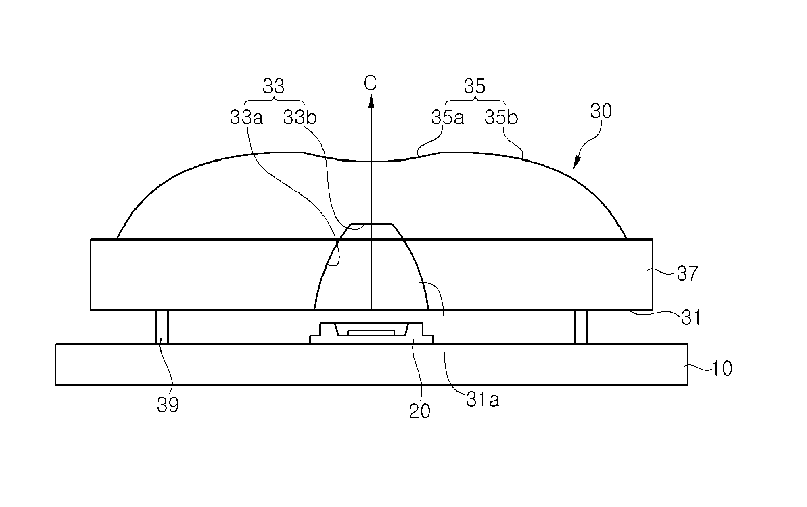
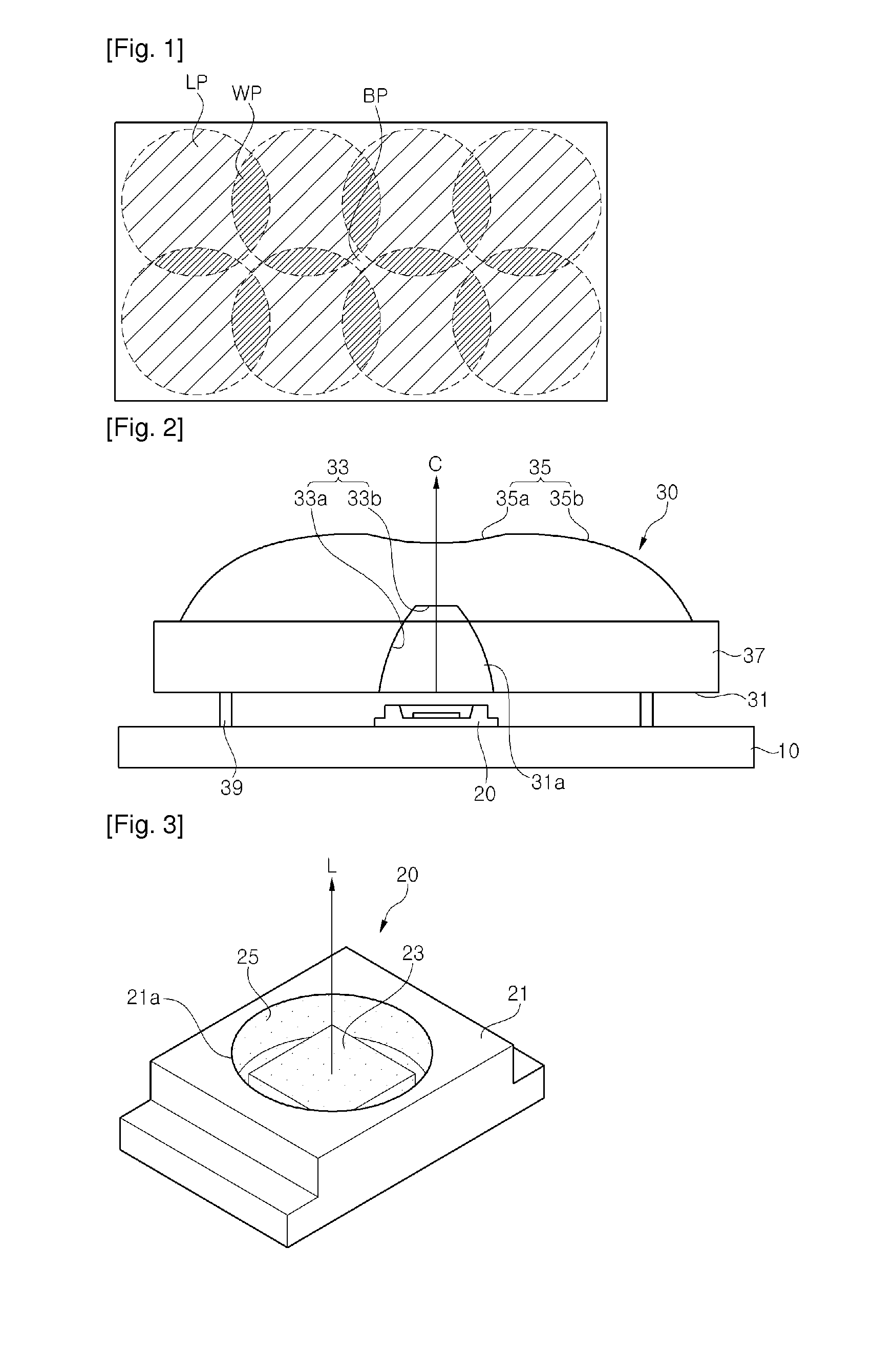
[0062]FIG. 2 is a schematic cross-sectional view for describing a light emitting module according to an embodiment of the present invention, and FIG. 3 is a perspective view for describing a light emitting device used in the light emitting module.

[0063]Referring to FIG. 2, the light emitting module includes a printed circuit board (PCB) 10, a light emitting device 20, and a lens 30. Although the PCB 10 is partially illustrated, a pl...


PUM


Abstract

A light emitting module including a lens is provided. The light emitting module includes a light emitting diode chip, and a lens. The lens according to an embodiment includes a lower surface having a concave portion, and an upper surface from which light incident on the concave portion is emitted. The upper surface of the lens includes a concave surface positioned in a central axis thereof. The concave portion of the lower surface includes at least one of a surface perpendicular to the central axis and a downwardly convex surface. At least one of the surface perpendicular to the central axis and the downwardly convex surface is positioned in a region narrower than an entrance region of the concave portion.

Description

CROSS-REFERENCE TO RELAYED APPLICATIONS[0001]This application is the National Stage of International Application No. PCT / KR2012 / 010314, filed on Nov. 30, 2012, and claims priority from and the benefit of Korean Patent Application No. 10-2011-0128375, filed on Dec. 2, 2011 and Korean Patent Application No. 10-2011-0141098, filed on Dec. 23, 2011, which are hereby incorporated by reference for all purposes as if fully set forth herein.BACKGROUND[0002]1. Field[0003]The present invention relates to a light emitting module, and more particularly, to a light emitting module including a lens for use as a surface illumination or a backlight of a liquid crystal display.[0004]2. Discussion of the Background[0005]There are edge-type backlights and direct-type backlights for backlighting a liquid crystal display. As for the edge-type backlights, light emitting diodes (LEDs) are arranged on a side of a light guide plate, and light incident from a light source backlights a liquid crystal panel by...

Claims


Application Information

Patent Timeline
Patent Type & Authority Applications(United States)
IPC IPC(8): F21K99/00F21V13/04F21V13/02F21V5/04
CPCF21K9/50F21K9/56F21Y2101/02F21V13/04F21V13/02F21V5/04F21V5/046H01L33/58G02B19/0066G02B5/021G02B5/0268G02B19/0028G02B19/0014F21K9/64F21Y2115/10F21K9/60F21V13/08F21V5/10
Inventor KIM, EUN JUKIM, BANG HYUNYANG, YOUNG EUN
Owner SEOUL SEMICONDUCTOR
Why Eureka
Try Eureka