Semiconductor Device Models Including Re-Usable Sub-Structures

a technology of semiconductors and substructures, applied in the field of metalrology systems and methods, can solve the problems of more difficult characterization, and more complex optical tools, and achieve the effects of less error-prone, computationally more efficient, and intuitiveness

Active Publication Date: 2015-07-16
KLA CORP
View PDF4 Cites 18 Cited by
  • Summary
  • Abstract
  • Description
  • Claims
  • Application Information

AI Technical Summary

Benefits of technology

[0014]In one aspect, a model building tool includes re-useable, parametric models of complex device sub-structures that are useable as building blocks in a model of a complex semiconductor device. This makes the model building process more intuitive and less error-prone. Furthermore, because the re-useable, parametric sub-structure models are optimized for specific structures and measurement applications, the resulting discretized measurement model is computationally more efficient than traditional models. In addition, the parametric sub-structure models can be saved and shared among different projects and different users.
[0015]In a further aspect, the re-useable, parametric sub-structure model is fully defined by the values of the independent parameters entered by the user of the model building tool. All other variables associated with the model shape and internal constraints among constituent geometric elements are pre-defined within the model. Thus, beyond the values of the independent parameters, no other user input is required to fully define the re-useable, parametric sub-structure model. This greatly simplifies the model building process.

Problems solved by technology

As devices (e.g., logic and memory devices) move toward smaller nanometer-scale dimensions, characterization becomes more difficult.
Devices incorporating complex three-dimensional geometry and materials with diverse physical properties contribute to characterization difficulty.
In response to these challenges, more complex optical tools have been developed.
Although models constructed from primitive structural building blocks offer a wide range of modeling flexibility and user control, the model building process becomes very complex and error prone when modeling complex device structures.
Accomplishing this is not an easy task, and users spend significant amounts of time ensuring that their models are correct.
In many cases, users do not realize their models are inconsistent and incorrect because it is difficult to comprehend how all of the primitive structural building blocks change shape and location in parameter space.
Specifically, it is very difficult to determine if models that are structurally consistent for a given set of parameter values remain structurally consistent for another set of parameter values.
This makes model-building very complex and prone to user errors.
Furthermore, model complexity makes it difficult for one user to understand models built by another.
The user needs to be able to understand the intent of the original model owner and this becomes increasingly challenging as the number of primitive structural building blocks, constraints, and independent parameters increases.
Consequently, transferring ownership of models (e.g., from applications engineers to process engineers) is a time consuming, difficult process.
In many cases, the complexity of the models leads to frustration amongst colleagues, and in some cases, prevents the transfer process from ever being fully completed.
However, with increasingly complicated models and less time per project, improved modeling methods and tools are desired.

Method used


Image

  • Semiconductor Device Models Including Re-Usable Sub-Structures
  • Semiconductor Device Models Including Re-Usable Sub-Structures
  • Semiconductor Device Models Including Re-Usable Sub-Structures

Examples


Embodiment Construction

[0034]Reference will now be made in detail to background examples and some embodiments of the invention, examples of which are illustrated in the accompanying drawings.

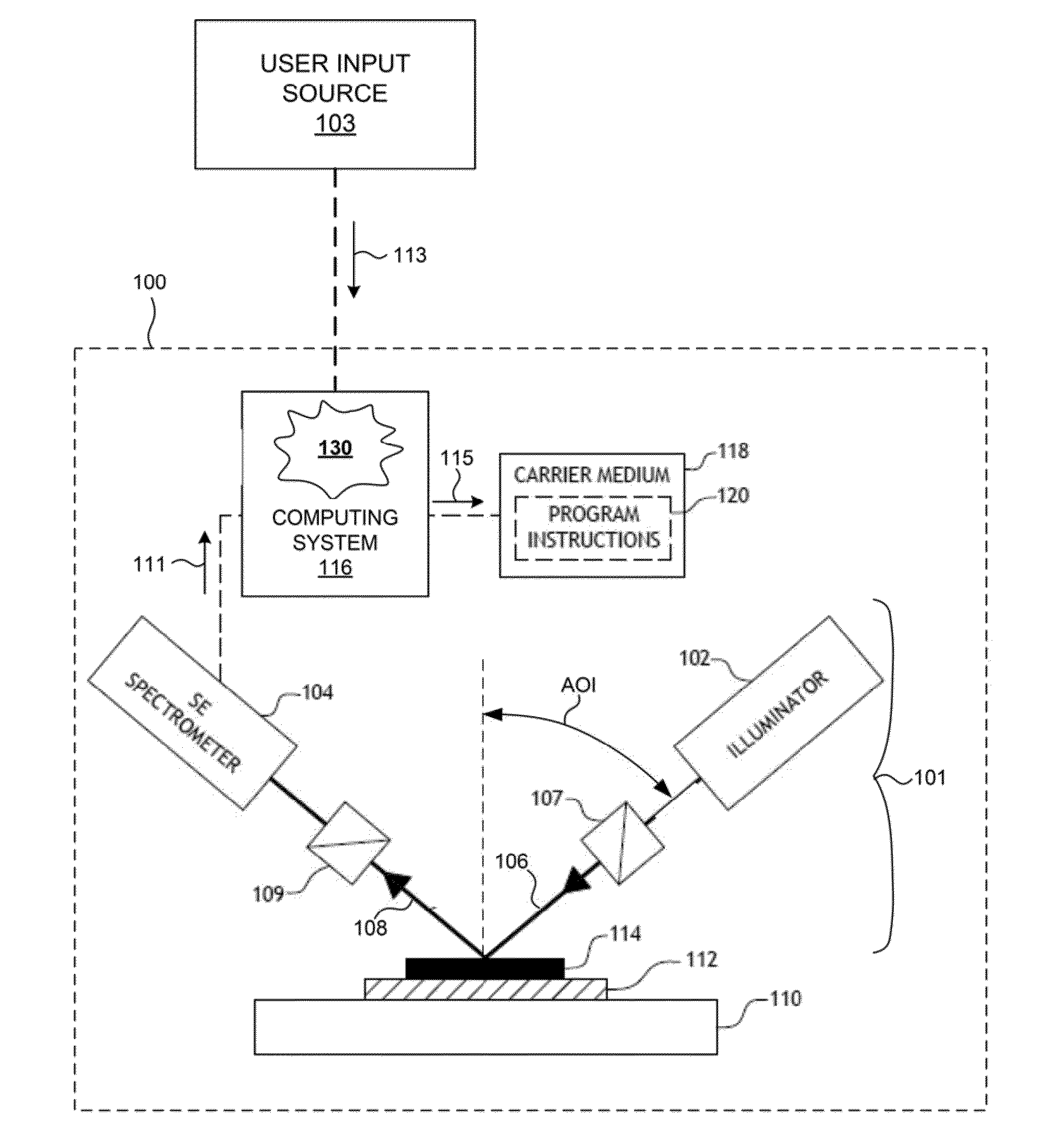
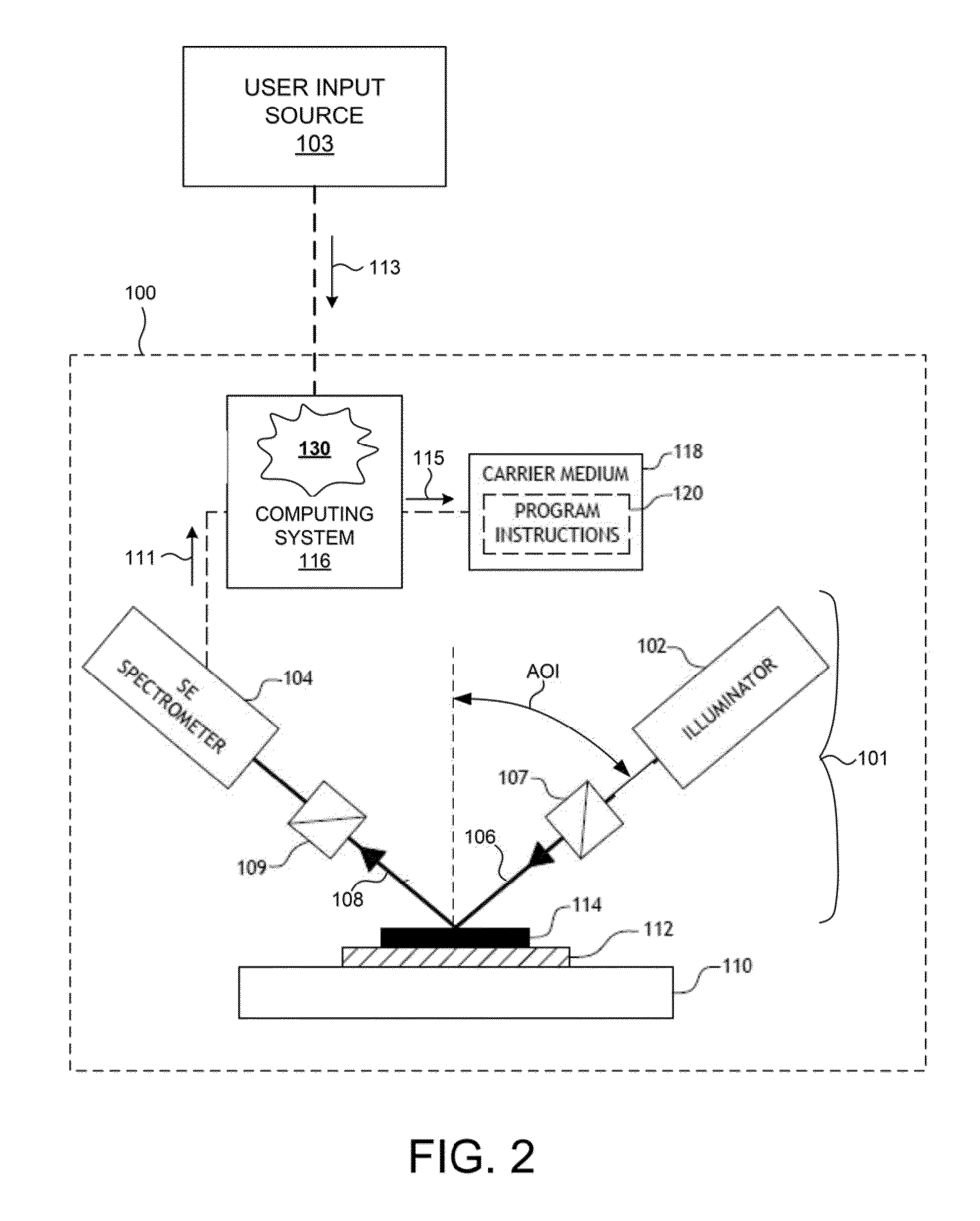
[0035]Methods and tools for generating measurement models of complex device structures based on re-useable, parametric models are presented. Metrology systems employing these models are configured to measure structural and material characteristics (e.g., material composition, dimensional characteristics of structures and films, etc.) associated with different semiconductor fabrication processes.

[0036]FIG. 2 illustrates a system 100 for measuring characteristics of a semiconductor wafer. As shown in FIG. 2, the system 100 may be used to perform spectroscopic ellipsometry measurements of one or more structures 114 of a semiconductor wafer 112 disposed on a wafer positioning system 110. In this aspect, the system 100 may include a spectroscopic ellipsometer equipped with an illuminator 102 and a spectrometer 104. The ill...


PUM


Abstract

Methods and tools for generating measurement models of complex device structures based on re-useable, parametric models are presented. Metrology systems employing these models are configured to measure structural and material characteristics associated with different semiconductor fabrication processes. The re-useable, parametric sub-structure model is fully defined by a set of independent parameters entered by a user of the model building tool. All other variables associated with the model shape and internal constraints among constituent geometric elements are pre-defined within the model. In some embodiments, one or more re-useable, parametric models are integrated into a measurement model of a complex semiconductor device. In another aspect, a model building tool generates a re-useable, parametric sub-structure model based on input from a user. The resulting models can be exported to a file that can be used by others and may include security features to control the sharing of sensitive intellectual property with particular users.

Description

CROSS REFERENCE TO RELATED APPLICATION[0001]The present application for patent claims priority under 35 U.S.C. §119 from U.S. provisional patent application Ser. No. 61 / 927,832, entitled “Building Optical Metrology Models Based on Structure and Application Delineated Characteristics,” filed Jan. 15, 2014, the subject matter of which is incorporated herein by reference in its entirety.TECHNICAL FIELD[0002]The described embodiments relate to metrology systems and methods, and more particularly to methods and systems for improved measurement accuracy.BACKGROUND INFORMATION[0003]Semiconductor devices such as logic and memory devices are typically fabricated by a sequence of processing steps applied to a specimen. The various features and multiple structural levels of the semiconductor devices are formed by these processing steps. For example, lithography among others is one semiconductor fabrication process that involves generating a pattern on a semiconductor wafer. Additional examples...

Claims


Application Information

Patent Timeline
Patent Type & Authority Applications(United States)
IPC IPC(8): G06F17/50
CPCG06F17/5045H01L22/12G01N21/211G01N21/9501H01L22/30G01N2021/213
Inventor ILORETA, JONATHANLAFFIN, MATTHEW A.POSLAVSKY, LEONIDKAACK, TORSTENZHAO, QIANGLEE, LIE-QUAN
Owner KLA CORP
Why Eureka
Try Eureka