
Nano-stamp and matched reader for Anti-counterfeiting applications

a technology of anti-counterfeiting applications and nano-stamps, which is applied in the validation field of security identification seals, can solve the problems of becoming more difficult for manufacturers to track products from the point of manufacture to the end user, and achieve the effect of high security and easy fabrication

Active Publication Date: 2015-07-30
XUV LASERS +1
View PDF10 Cites 7 Cited by
  • Summary
  • Abstract
  • Description
  • Claims
  • Application Information

AI Technical Summary

Benefits of technology

The present invention provides a way to verify the authenticity of a part by using a nano-stamp that generates a unique pattern when interrogated with near infrared, visible, or ultraviolet light. This pattern is invisible to the eye and difficult to replicate or alter, making it highly secure. The nano-stamp can be easily fabricated using compact, table-top extreme ultraviolet lasers. This invention overcomes the limitations of previous methods and provides a more effective way to verify the authenticity of parts.

Problems solved by technology

Due to increased globalization, manufacturing delocalization, sophisticated supply chains and complex distribution models, it has become more difficult for manufacturers to track products from the point of manufacture to end-user.

Method used


Image

  • Nano-stamp and matched reader for Anti-counterfeiting applications
  • Nano-stamp and matched reader for Anti-counterfeiting applications
  • Nano-stamp and matched reader for Anti-counterfeiting applications

Examples


example

Observation Of A Unique Far-Field Reflection Pattern From A Nano-Stamp:

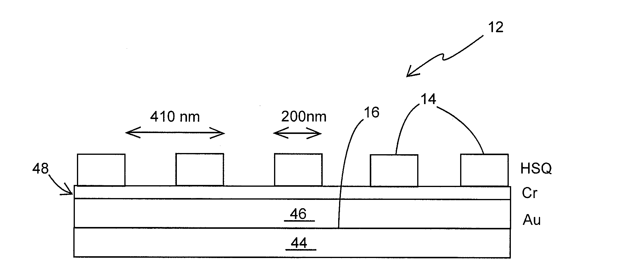
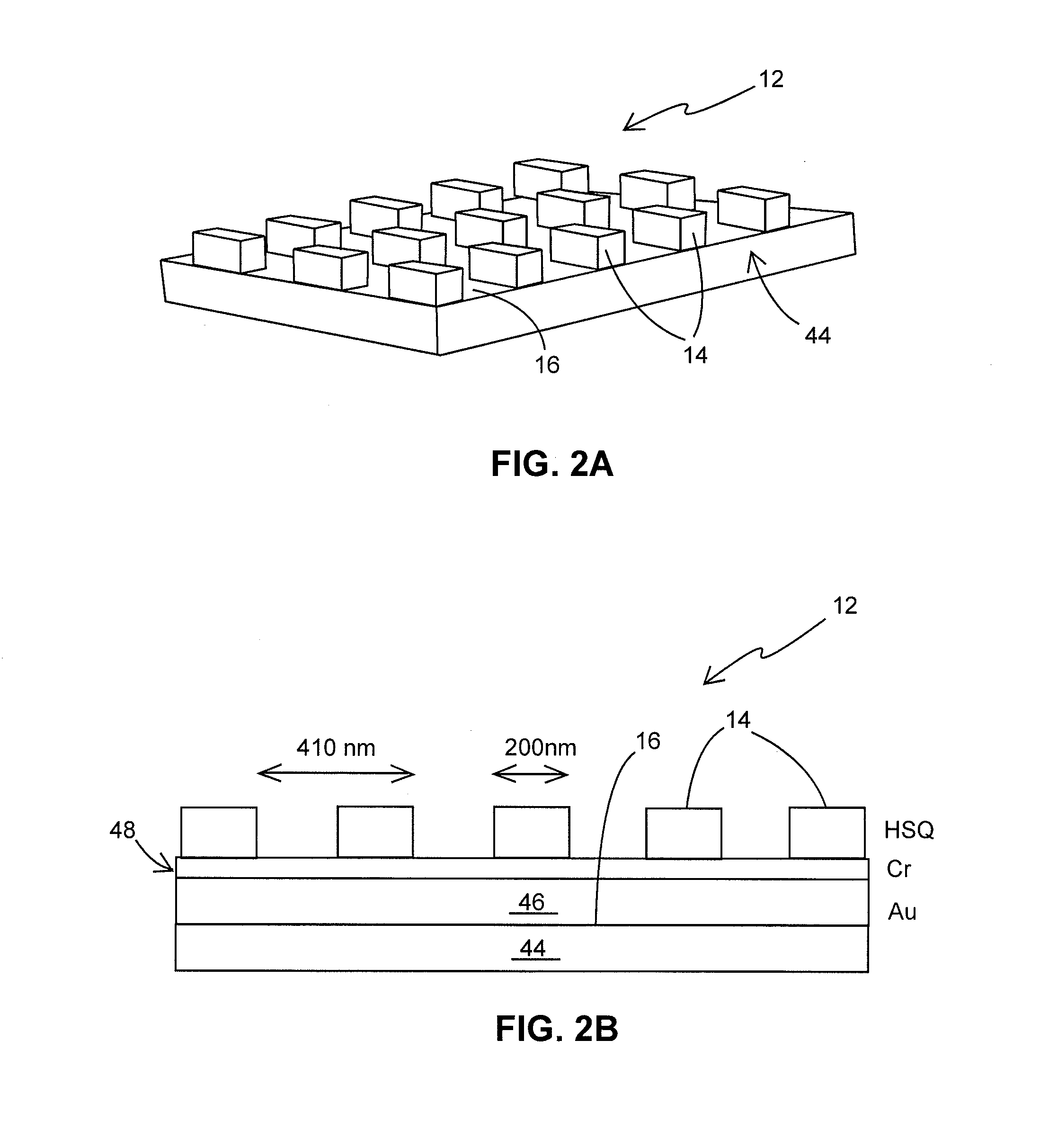
[0030]Turning now to FIGS. 2A and 2B, shown is nano-stamp 12 fabricated on a Si substrate, 44, covered by 160 nm of Au, 46, 10 nm of Cr, 48, on surface 16, followed by a patterned layer of hydrogen silsesquioxane (HSQ) cured photoresist. The HSQ has similar optical characteristics to SiO2. Nano-stamp 12 was patterned 14 by Talbot imaging of a mask using an extreme ultraviolet (EUV) light (46.9 nm) capillary discharge laser, whereby a pattern virtually free of defects was generated within its entire area. The mask was a 100 nm thick Si membrane covered with 80 nm of HSQ, and squares were generated thereon using e-beam lithography. Substrate 44 for nano-stamp 12 was located in the first Talbot plane of the mask. Talbot lithography produces one to one replicas of the mask.

[0031]Pattern 14 in nano-stamp 12 included 200 nm×200 nm rectangular HSQ pillars having a height of 120 nm and a periodicity of 410 nm, as an exam...


PUM


Abstract

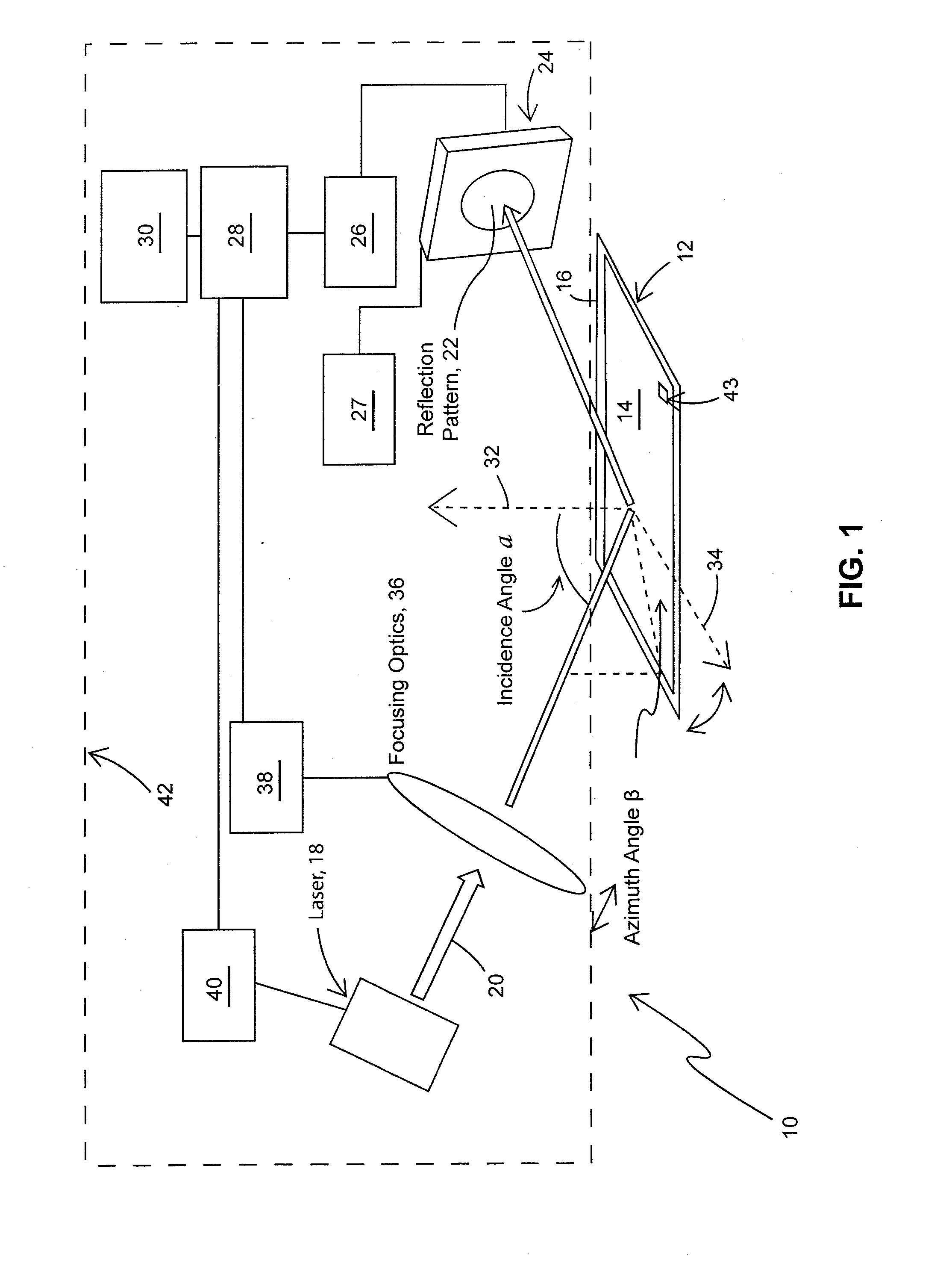
A method and system for reading a security seal having a unique far-field pattern are described. Periodic nano-structure is generated on the surface of a substrate having spacings of hundreds of nanometers, or smaller, and affixed on a product, or generated directly onto the product. A laser beam having a wavelength longer than the periodic spacings directed onto at least a portion of the surface of the substrate at a chosen angle of incidence and a selected azimuthal angle relative to a chosen direction produces a unique far-field pattern that may be imaged by a digital image detector disposed at a chosen distance from the illuminated region, compared with a stored reference, and validated. The nanoscale sub-wavelength patterns can be printed using extreme ultraviolet light and read with readily available visible or ultraviolet light. The security seal contains a pattern that is invisible to the eye and to an optical microscope. Brand protection at different stages of the life-span of a product, from production to purchase is therefore available.

Description

CROSS-REFERENCE TO RELATED APPLICATIONS[0001]The present application claims the benefit of U.S. Provisional Patent Application No. 61 / 915,761 for “Method For Creating A Nano-Stamp And A Matched Reader For Anti-Counterfeiting Applications,” by Mario C. Marconi et al., which was filed on Dec. 13, 2013, the contents of which application is hereby specifically incorporated by reference herein for all that it discloses and teaches.FIELD OF THE INVENTION[0002]The present invention relates generally to validation of security identification seals and, more particularly, to an apparatus and method including a nano-structured surface, which upon interrogation using near infrared, visible or ultraviolet light generates a unique, far-field reflection pattern, which is validated using a reader adapted for this purpose that reveals the existence of the seal without revealing its geometry, creating thereby a high level of security.BACKGROUND OF THE INVENTION[0003]The annual global trade in illegit...

Claims


Application Information

Patent Timeline
Patent Type & Authority Applications(United States)
IPC IPC(8): G06Q30/00
CPCG06Q30/0185B42D25/41G07D7/12G07D7/003B42D25/29B42D25/328
Inventor MARCONI, MARIO C.MENONI, CARMEN S.ROCCA, JORGE J.
Owner XUV LASERS
Learn More