Semiconductor package having a dissipating plate

a technology of dissipating plate and semiconductor, which is applied in the direction of solid-state devices, basic electric elements, electrical apparatus construction details, etc., can solve the problems of cracks on and achieve the effect of increasing the dissipation efficiency of a single chip packag

Inactive Publication Date: 2015-08-06
SAMSUNG ELECTRONICS CO LTD
View PDF8 Cites 37 Cited by
  • Summary
  • Abstract
  • Description
  • Claims
  • Application Information

AI Technical Summary

Benefits of technology

[0030]Thus, an LMTIM instead of an HMTIM may be used for manufacturing the semiconductor package irrespective of a single package and a stack package, which may standardize the packaging process for manufacturing a semiconductor package. In addition, the dissipating efficiency of a single chip package may be increased by replacing a conventional HMTIM with an LMTIM.

Problems solved by technology

However, HMTIM may cause cracks on a single chip package due to the high modulus thereof.
Various scratches and dents may be generated on the top surface of a single chip package in a packaging process and the scratches and dents are usually formed into the cracks in a subsequent process due to the high modulus of the HMTIM.

Method used


Image

  • Semiconductor package having a dissipating plate
  • Semiconductor package having a dissipating plate
  • Semiconductor package having a dissipating plate

Examples


Embodiment Construction

[0037]Various exemplary embodiments will be described more fully hereinafter with reference to the accompanying drawings, in which some exemplary embodiments are shown. The present invention may, however, be embodied in many different forms and should not be construed as limited to the exemplary embodiments set forth herein. In the drawings, the sizes and relative sizes of layers and regions may be exaggerated for clarity.

[0038]It will be understood that when an element or layer is referred to as being “on,”“connected to” or “coupled to” another element or layer, it can be directly on, connected or coupled to the other element or layer or intervening elements or layers may be present. Like numerals may refer to like elements throughout.

[0039]Hereinafter, exemplary embodiments will be explained in detail with reference to the accompanying drawings.

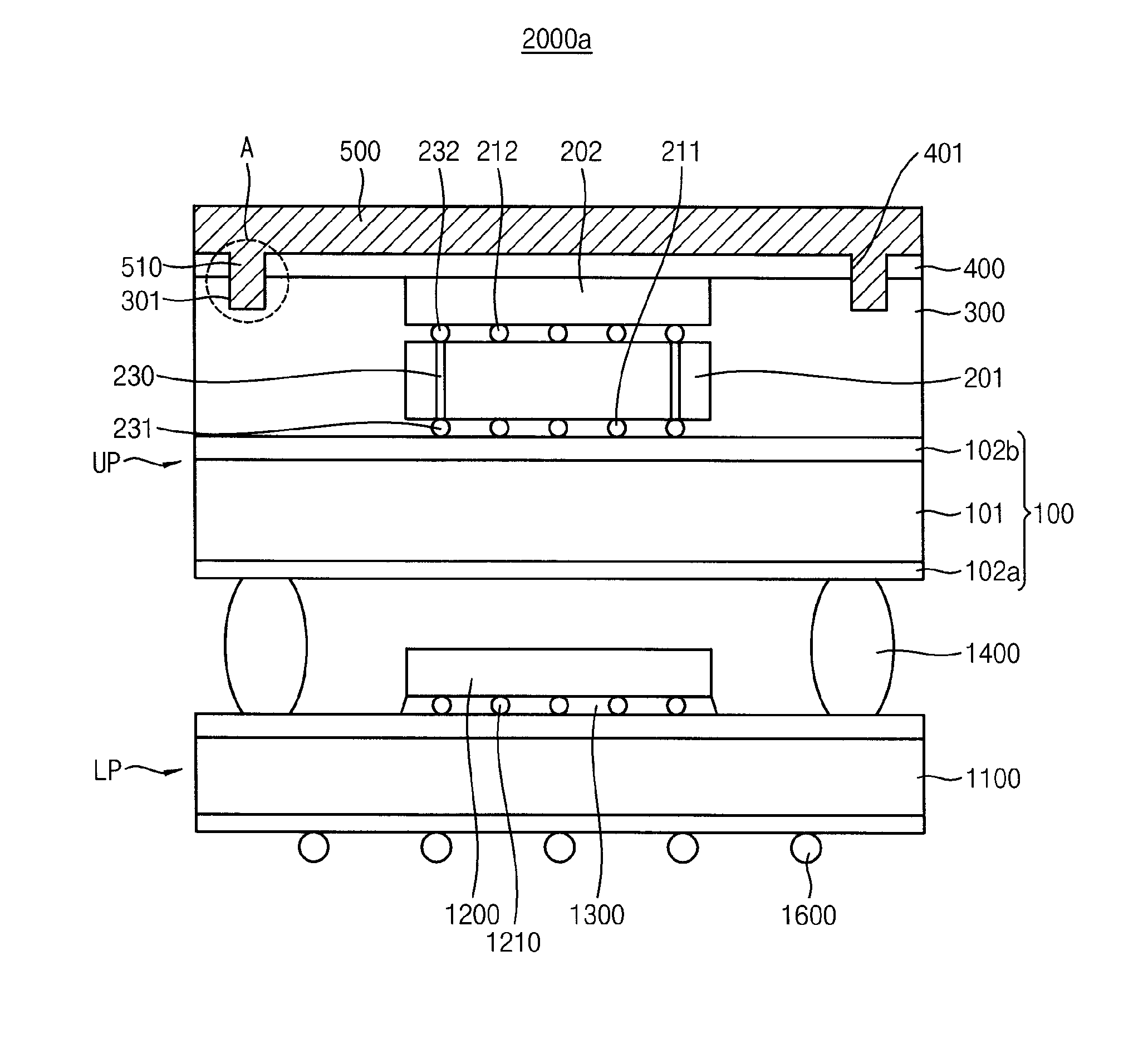
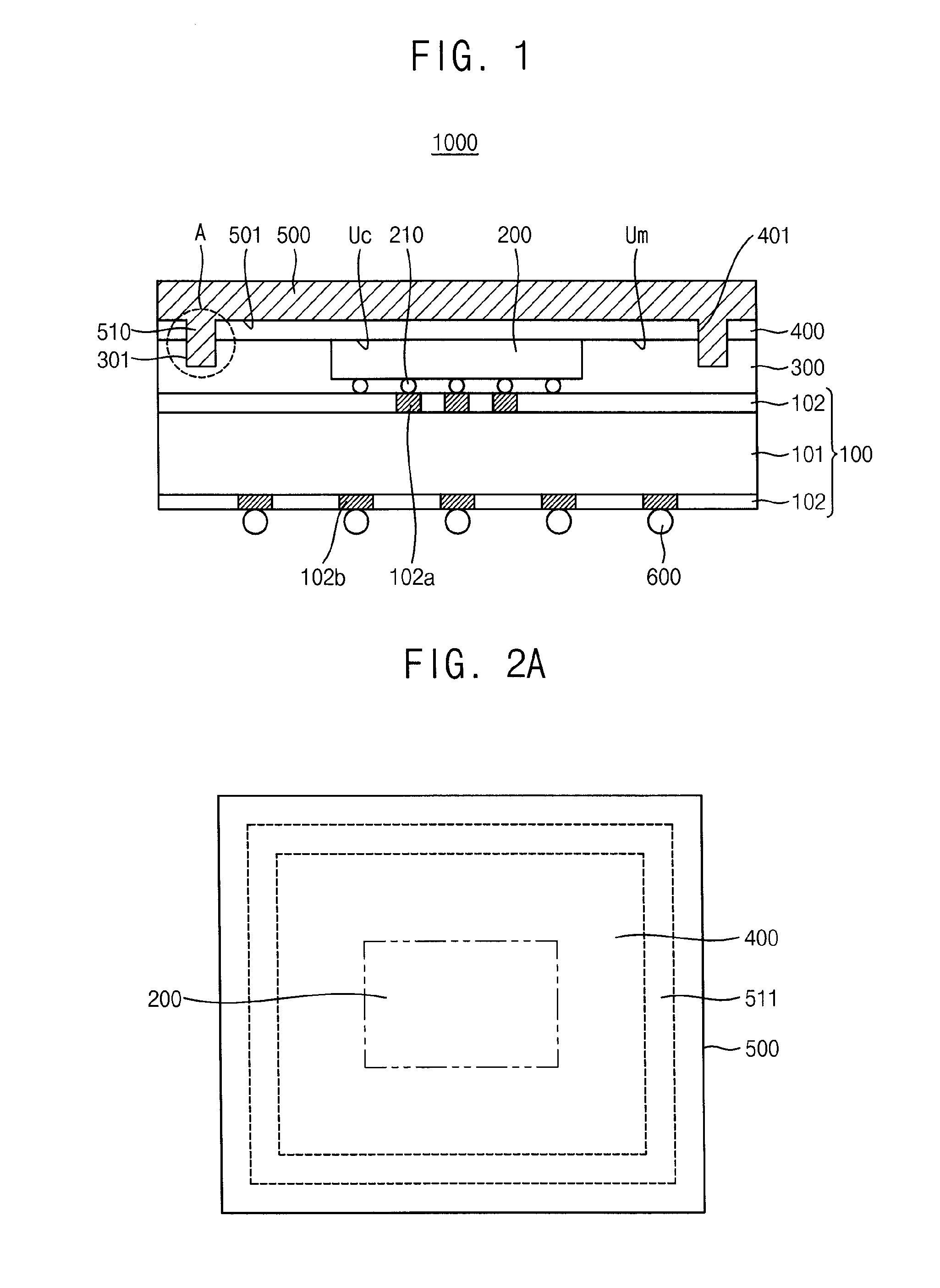
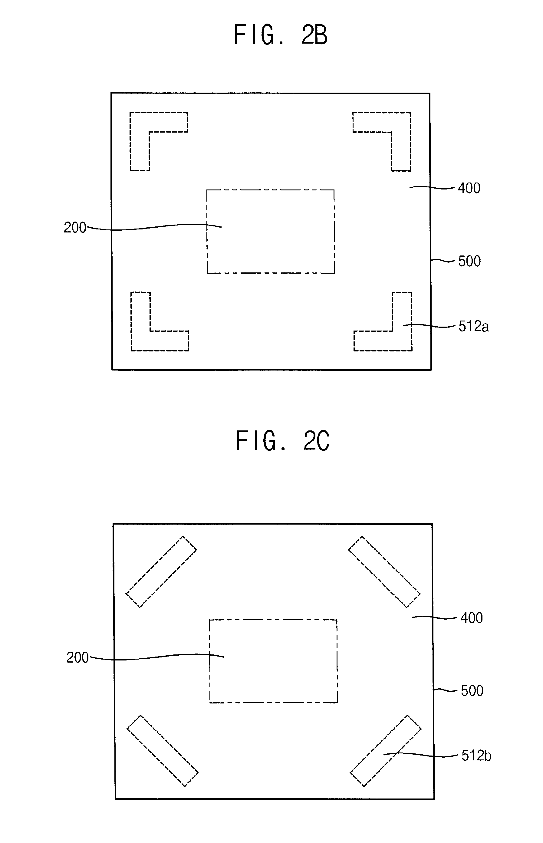
[0040]FIG. 1 is a structural view of a semiconductor package in accordance with an exemplary embodiment of the present inventive concept. ...


PUM


Abstract

A semiconductor package includes an integrated circuit device on a circuit board, a mold layer covering the integrated circuit board, a dissipating plate that dissipates heat from the integrated circuit device and a thermal conductive adhesive having a thermal interface material (TIM). The dissipating plate includes at least one protrusion protruding from a peripheral portion of the bottom of the dissipating plate that is inserted into the mold layer around the integrated circuit device. The dissipating plate is primarily secured to the mold layer by the protrusion, not by the thermal conductive adhesive. The thermal conductive adhesive includes a low modulus TIM (LMTIM) that supplementally adheres the dissipating plate to the mold layer.

Description

CROSS-REFERENCE TO RELATED APPLICATIONS[0001]This application claims priority under 35 U.S.C §119 from Korean Patent Application No. 10-2014-0012670 filed on Feb. 4, 2014 in the Korean Intellectual Property Office, and all the benefits accruing therefrom, the contents of which are herein incorporated by reference in their entirety.BACKGROUND[0002]1. Field[0003]Exemplary embodiments are directed to a semiconductor package, and more particularly, to a semiconductor package having a dissipating plate such as a heat slug.[0004]2. Description of the Related Art[0005]As recent electronic devices have been more highly integrated with improved performance, semiconductor packages are also manufactured to be smaller denser. Higher performance from high density semiconductor packages at higher speeds necessarily generates more heat in the semiconductor package. Thus, sufficient thermal dissipation becomes a useful factor for increasing the operation stability and product reliability of a semic...

Claims


Application Information

Patent Timeline
Patent Type & Authority Applications(United States)
IPC IPC(8): H01L25/18H05K7/20H01L25/065H01L23/31H01L23/367H01L23/00H05K7/02H01L23/12
CPCH01L2924/1434H01L2924/1431H01L2224/16227H01L2224/16057H01L2224/32245H01L2225/06513H01L2225/06517H01L2225/06541H01L2225/06589H01L2225/06586H01L25/18H05K7/023H05K7/20409H01L23/12H01L23/3107H01L23/3675H01L24/17H01L24/32H01L25/0657H01L2224/16113H01L2224/17517H01L25/105H01L2224/13025H01L2224/16145H01L2224/16146H01L2224/16225H01L2224/17181H01L2224/32225H01L2224/73204H01L2224/73253H01L2225/1023H01L2225/1058H01L2225/1094H01L2924/15311H01L2924/15331H01L2225/06565H01L23/367H01L23/4334H01L23/49811H01L23/49827H01L2924/181H01L2924/12042H01L23/3128H01L2924/00
Inventor CHUN, HYUN-SUKKIM, MIN
Owner SAMSUNG ELECTRONICS CO LTD
Why Eureka
Try Eureka