Covering method and organic el element manufacturing method

a manufacturing method and organic el technology, applied in the direction of organic semiconductor devices, semiconductor/solid-state device testing/measurement, electrical or functional layers with local level unevenness, etc., can solve the problems of forming dark spots, affecting the and affecting the stability of the organic el element, etc., to achieve the effect of high boiling point, not easy to evaporate, and increased viscosity of the mixtur

Active Publication Date: 2015-08-06
JOLED INC
View PDF3 Cites 14 Cited by
  • Summary
  • Abstract
  • Description
  • Claims
  • Application Information

AI Technical Summary

Benefits of technology

[0012]The covering method pertaining to one aspect of the present disclosure involves the use of a solvent that has a high boiling point and thus does not evaporate easily. Due to this, the viscosity of the mixture increases only by a small degree in the course of time, and thus the mixture has high stability. Further, the high concentration of solid content in the mixture provides the mixture with high viscosity. Due to this, the mixture, when applied with respect to the defective portion, does not spread easily. As such, the covering

Problems solved by technology

Also, resist defect may result in an electrode or a functional layer having a surface with local level unevenness.
Further, there may even be cases where the functional layer above the elect

Method used


Image

  • Covering method and organic el element manufacturing method
  • Covering method and organic el element manufacturing method
  • Covering method and organic el element manufacturing method

Examples


embodiment 1

[1.1 Overall Structure]

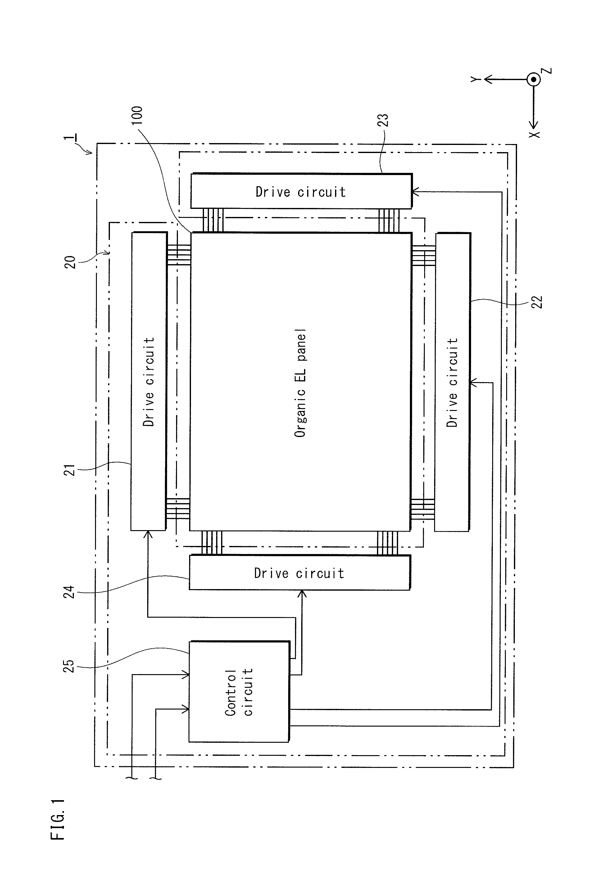
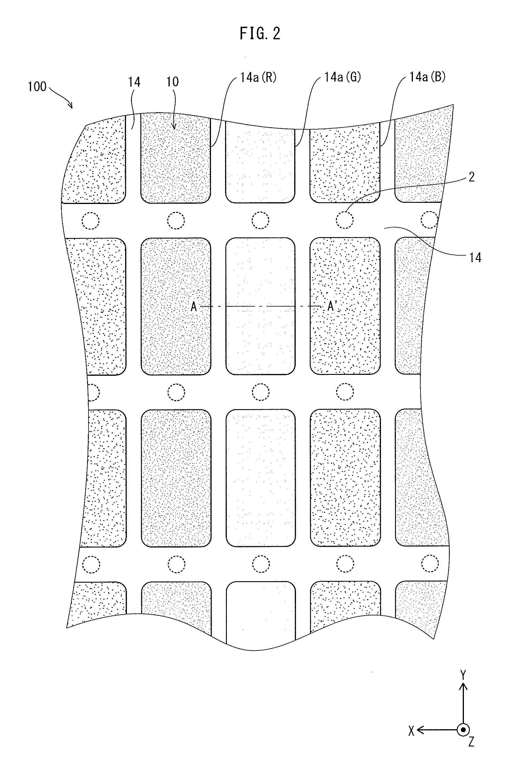
[0032]FIG. 1 is a schematic block diagram illustrating a structure of an organic EL display device 1. The organic EL display device 1 includes an organic EL display panel 100 pertaining to embodiment 1. As illustrated in FIG. 1, the organic EL display device 1 includes the organic EL display panel 100 and a drive / control unit 20 connected to the organic EL display panel 100. The organic EL display panel 100 is a panel utilizing electro-luminescence occurring in organic material. The organic EL display panel 100 includes a plurality of organic EL elements 10 (illustrated in FIGS. 2 and 3) that are disposed on a substrate and arranged, for example, to form a matrix. The drive / control unit 20 includes four drive circuits, namely drive circuits 21 through 24, and a control circuit 25.

[0033]Note that when the organic EL display device 1 is actually implemented, the arrangement of the drive / control unit 20 with respect to the organic EL display panel 100 may differ ...

embodiment 2

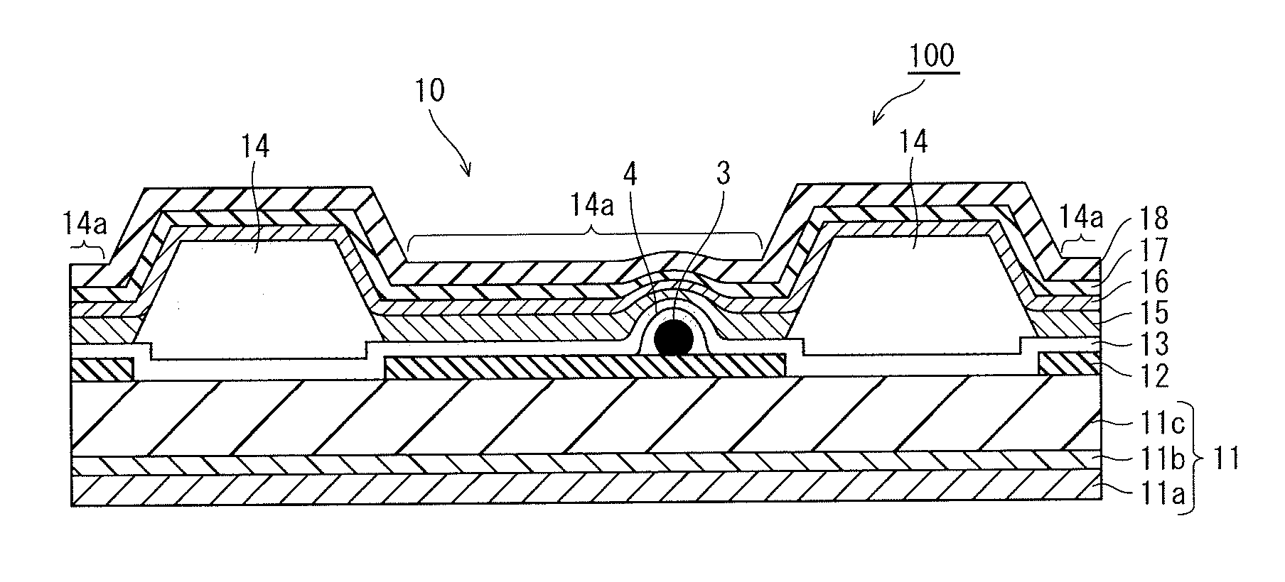
[0124]In embodiment 1, the defective portion 3 is a foreign particle on the pixel electrode 12. However, the defective portion 3 need not be such a foreign particle. For example, as already described in embodiment 1 in the explanation concerning the defective portion 3, an upward protrusion may be formed in the pixel electrode 12 due to a foreign particle or an upward protrusion existing lower than the pixel electrode 12, in which case the upward protrusion of the pixel electrode 12 is the defective portion 3.

[0125]In embodiment 2, description is provided on a case where the defective portion 3 is an upward protrusion of the pixel electrode 12 that is formed due to an upward protrusion formed in the surface of the interlayer insulating layer 11c.

[0126]Note that in the following, in order to avoid the repetition of description already provided in embodiment 1, constituent elements that correspond to those having been described in embodiment 1 are provided with the same reference sig...

embodiment 3

[0131]In embodiment 1, the defective portion 3 is a foreign particle on the pixel electrode 12. In embodiment 2, the defective portion 3 is an upward protrusion of the pixel electrode 12 that is formed due to an upward surface protrusion existing lower the pixel electrode 12. However, the defective portion 3 need not be such a foreign particle or such an upward protrusion. For example, the defective portion 3 may be a downward protrusion.

[0132]FIGS. 10A-10C are cross-sectional views schematically illustrating an overview of a covering method for covering the defective portion 3 in an organic EL element pertaining to embodiment 3. FIG. 10A illustrates a state before the mixture 40 is applied with respect to the defective portion 3. FIG. 10B illustrates a state where the tip portion 33a of the needle 33 is in contact with the defective portion 3. FIG. 10C illustrates a state where the tip portion 33a of the needle 33 has been moved away from the defective portion 3 and the defective p...


PUM


Abstract

A covering method including: preparing a mixture containing insulative material and a solvent; applying the mixture over a defective portion; and covering the defective portion with the insulative material by causing the solvent to evaporate from the mixture. In the covering method, the solvent has a boiling point no lower than 178 degrees Celsius, and in the mixture, a weight ratio percentage of the insulative material to the solvent is no lower than 10%. Thus, the defective portion, which may result in a dark spot, can be efficiently covered with insulative material while ensuring that a non-light-emission area that is formed accordingly has the smallest-necessary size and that sufficient insulation is achieved.

Description

TECHNICAL FIELD[0001]The present disclosure relates to a covering method of covering a defective portion of an organic electro-luminescence (EL) element, and a manufacturing method of manufacturing an organic EL element.BACKGROUND ART[0002]Recently, organic EL display panels are gaining popularity as display devices. A typical organic EL display panel includes a substrate and organic EL elements disposed on the substrate. An organic EL display panel realizes high visibility and high shock resistance, because the organic EL elements included therein have high visibility for being self-luminescent and have high shock resistance for having a fully solid-state structure.[0003]An organic EL element is a current-driven light-emission element. An organic EL element typically includes an electrode pair composed of a pixel electrode and a common electrode, and a plurality of functional layers that are layered between the pixel electrode and the common electrode. The functional layers include...

Claims


Application Information

Patent Timeline
IPC IPC(8): H01L27/32H01L51/52H01L21/66H01L51/56
CPCH01L2251/568H01L27/3244H01L51/56H01L27/3258H01L51/5253H01L22/26H01L22/20H10K59/12H10K71/861H10K59/124H10K50/844H10K71/00
Inventor SHIMAMURA, TAKAYUKISANO, ASAKIMATSUSHIMA, HIDEAKIISHIKURA, NOBUYUKI
Owner JOLED INC
Why Eureka
Try Eureka