Bipolar transistor with carbon alloyed contacts

Inactive Publication Date: 2015-08-20
IBM CORP
View PDF2 Cites 4 Cited by
  • Summary
  • Abstract
  • Description
  • Claims
  • Application Information

AI Technical Summary

Benefits of technology

The patent describes a method for forming a bipolar junction transistor and a device that includes a collector intrinsic region, an emitter intrinsic region, and an intrinsic base region. Carbon is introduced into at least one of the collector extrinsic region, the emitter extrinsic region, and the base extrinsic region to suppress the diffusion of dopants into the intrinsic base region. The technical effect of this patent is the improvement of the performance and reliability of bipolar junction transistors by preventing dopant diffusion during the process while ensuring electrical connections between the collector, emitter, and base regions.

Problems solved by technology

Diffusion of impurities is in nano-scale devices is a challenge.

Method used


Image

  • Bipolar transistor with carbon alloyed contacts
  • Bipolar transistor with carbon alloyed contacts
  • Bipolar transistor with carbon alloyed contacts

Examples


Embodiment Construction

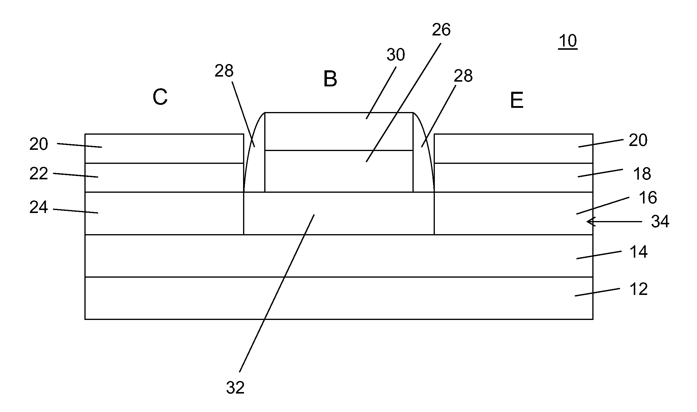
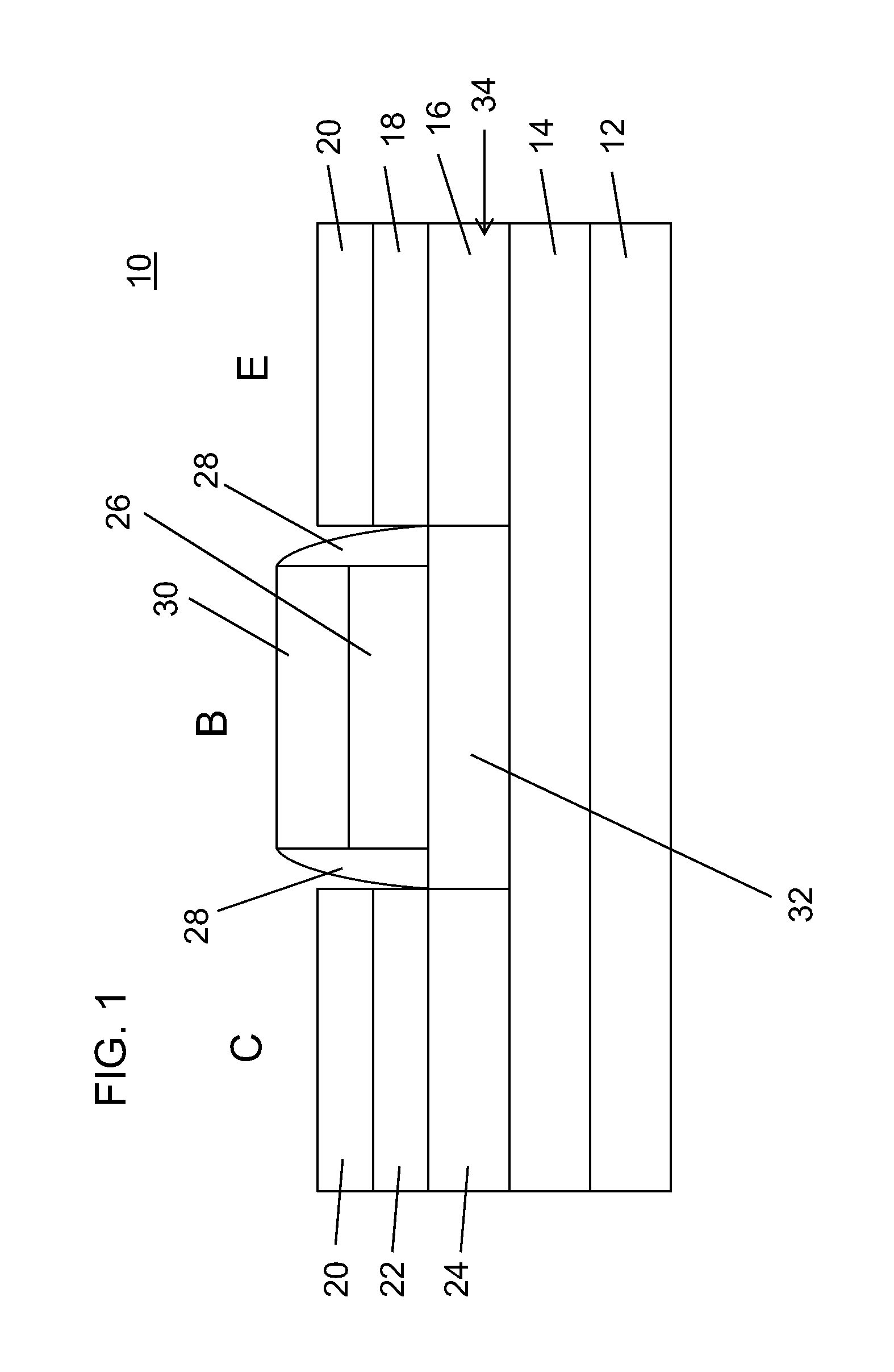
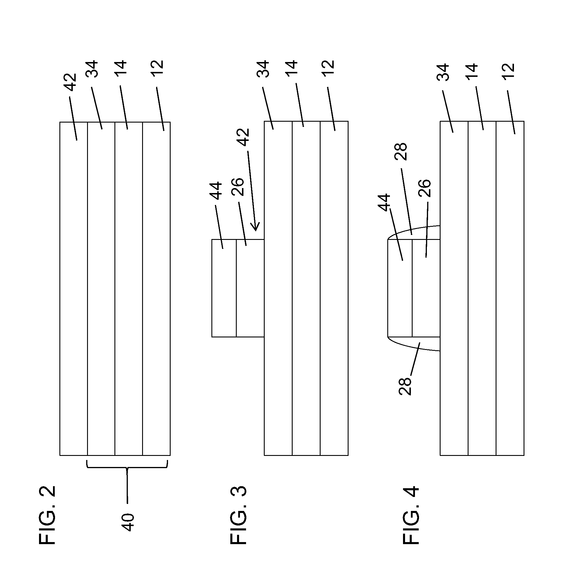
[0020]In accordance with the present principles, bipolar transistor devices are provided wherein at least one of an extrinsic base, collector or emitter region includes carbon (preferably less than about 5 atomic percent) to suppress the diffusion of impurities. In some embodiments, intrinsic emitter and / or collector regions may also include carbon (preferably less than about 1 atomic percent). Methods for fabricating the bipolar transistor devices in accordance with the present principles are also described.

[0021]It is to be understood that the present invention will be described in terms of a given illustrative architecture on a wafer or substrate; however, other architectures, structures, substrates, materials and process features and steps may be varied within the scope of the present invention.

[0022]It will also be understood that when an element such as a layer, region or substrate is referred to as being “on” or “over” another element, it can be directly on the other element ...


PUM


Abstract

A method for forming a bipolar junction transistor includes forming a collector intrinsic region, an emitter intrinsic region and an intrinsic base region between the collector intrinsic region and the emitter intrinsic region. A collector extrinsic contact region is formed in direct contact with the collector intrinsic region; an emitter extrinsic contact region is formed on the emitter intrinsic region and a base extrinsic contact region is formed in direct contact with the intrinsic base region. Carbon is introduced into at least one of the collector extrinsic contact region, the emitter extrinsic contact region and the base extrinsic contact region to suppress diffusion of dopants into the junction region.

Description

BACKGROUND[0001]1. Technical Field[0002]The present invention relates to transistor devices and methods for formation, and more particularly to bipolar transistors with carbon alloyed contacts.[0003]2. Description of the Related Art[0004]Diffusion of impurities is in nano-scale devices is a challenge. In nano-scale devices including transistors, such as lateral bipolar junction transistors (BJTs), diffusion of impurities must be suppressed to avoid junction widening. For example, in a lateral n-p-n BJT, phosphorous or other n-type impurities may diffuse from an n+ doped emitter and / or collector regions into to a p-type base and compromise the doping of the base region (reduce or counter-dope). Similarly, in a p-n-p device, phosphorous or other n-type impurity may diffuse from n+ doped extrinsic base into the n-type intrinsic base. The same applies to the diffusion of p-type impurities, such as, boron.SUMMARY[0005]A method for forming a bipolar junction transistor includes forming a ...

Claims


Application Information

Patent Timeline
IPC IPC(8): H01L29/08H01L29/732H01L29/66
CPCH01L29/167H01L29/66272H01L29/732H01L29/0821H01L29/66287H01L29/0826H01L29/0804H01L29/0808H01L29/1004H01L29/66234H01L29/735H01L27/06H01L27/0623H01L29/0638H01L29/0649H01L29/41708H01L29/42304H01L29/6625H01L29/7398
Inventor CHAN, KEVIN K.HEKMATSHOARTABARI, BAHMANNING, TAK H.
Owner IBM CORP
Why Eureka
Try Eureka