Device with Transparent and Higher Conductive Regions in Lateral Cross Section of Semiconductor Layer

a technology of semiconductor layer and lateral cross section, applied in the field of emitting devices, can solve the problems of high gallium content and uneven incorporation of aluminum in the algan layer, and achieve the effects of low light absorption, higher conduction, and high transmission coefficien

Active Publication Date: 2015-09-10
SENSOR ELECTRONICS TECH
View PDF0 Cites 10 Cited by
  • Summary
  • Abstract
  • Description
  • Claims
  • Application Information

AI Technical Summary

Benefits of technology

[0012]In light of the above, the inventors recognize that compositional and / or doping inhomogeneities allow for the development of conduction channels, e.g., in p-type superlattice layers. At the same time, the regions high in aluminum content allow for low light absorption (e.g., a higher transmission coefficient). The inventors propose to achieve a desired balance of higher conduction with reduced light absorption by tailoring semiconductor properties through the use of composite inhomogeneities, thereby obtaining a more optimal semiconductor material for light emitting / transmission applications.

Problems solved by technology

With proper growth conditions, it also was found that the aluminum did not incorporate uniformly throughout the AlGaN layer (i.e., the material has areas of high and low concentrations of aluminum spread throughout).
These defects have high gallium content.

Method used


Image

  • Device with Transparent and Higher Conductive Regions in Lateral Cross Section of Semiconductor Layer
  • Device with Transparent and Higher Conductive Regions in Lateral Cross Section of Semiconductor Layer
  • Device with Transparent and Higher Conductive Regions in Lateral Cross Section of Semiconductor Layer

Examples


Embodiment Construction

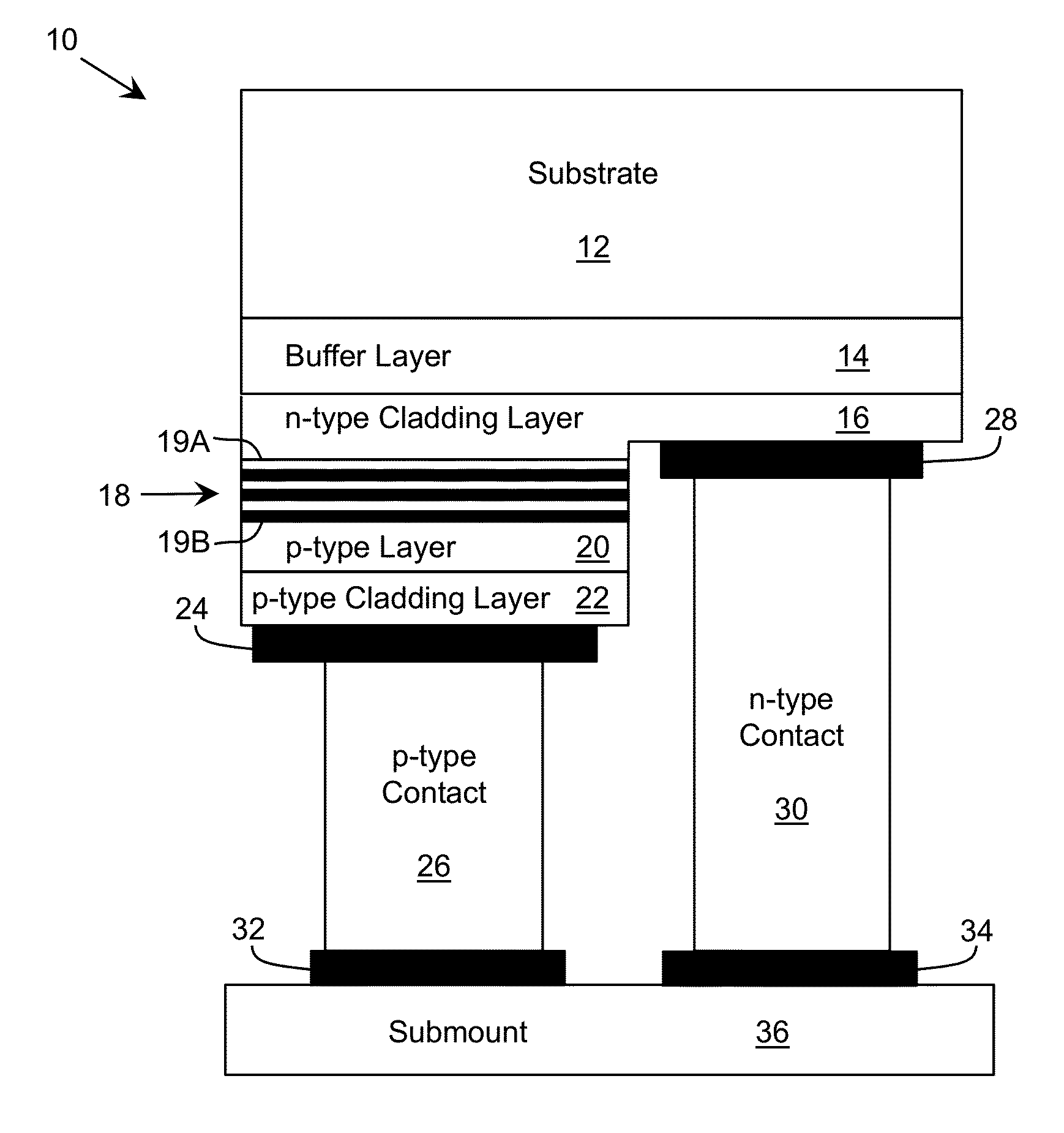
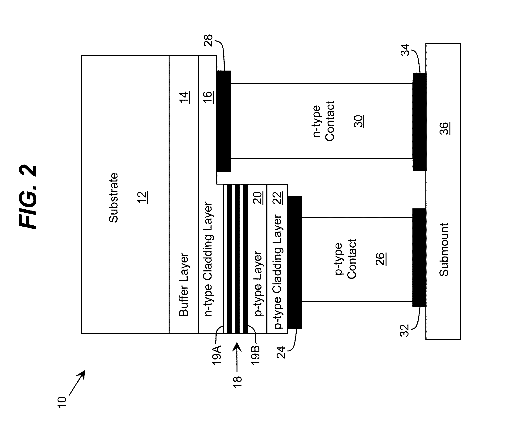
[0046]As indicated above, aspects of the invention provide a device including one or more layers with lateral regions configured to facilitate the transmission of radiation through the layer and lateral regions configured to facilitate current flow through the layer. The layer can comprise a short period superlattice, which includes barriers alternating with wells. In this case, the barriers can include both transparent regions, which are configured to reduce an amount of radiation that is absorbed in the layer, and higher conductive regions, which are configured to keep the voltage drop across the layer within a desired range. As used herein, unless otherwise noted, the term “set” means one or more (i.e., at least one) and the phrase “any solution” means any now known or later developed solution.

[0047]Turning to the drawings, FIG. 2 shows a schematic structure of an illustrative emitting device 10 according to an embodiment. In a more particular embodiment, the emitting device 10 i...


PUM


Abstract

A device including one or more layers with lateral regions configured to facilitate the transmission of radiation through the layer and lateral regions configured to facilitate current flow through the layer is provided. The layer can comprise a short period superlattice, which includes barriers alternating with wells. In this case, the barriers can include both transparent regions, which are configured to reduce an amount of radiation that is absorbed in the layer, and higher conductive regions, which are configured to keep the voltage drop across the layer within a desired range.

Description

REFERENCE TO RELATED APPLICATIONS[0001]The current application claims the benefit of U.S. Provisional Application No. 62 / 090,101, which was filed on 10 Dec. 2014. The current application is also a continuation-in-part of U.S. application Ser. No. 14 / 531,162, which was filed on 3 Nov. 2014, which is a continuation of U.S. application Ser. No. 14 / 184,649, titled “Emitting Device with Compositional and Doping Inhomogeneities in Semiconductor Layers,” which was filed on 19 Feb. 2014, which claims the benefit of U.S. Provisional Application No. 61 / 768,692, titled “Emitting Device with Compositional and Doping Inhomogeneities in Semiconductor Layers,” which was filed on 25 Feb. 2013, and which is a continuation-in-part of U.S. application Ser. No. 13 / 572,446, titled “Emitting Device with Compositional and Doping Inhomogeneities in Semiconductor Layers,” which was filed on 10 Aug. 2012, and which claims the benefit of U.S. Provisional Application No. 61 / 522,425, titled “Light Emitting Diod...

Claims


Application Information

Patent Timeline
Patent Type & Authority Applications(United States)
IPC IPC(8): H01L33/06H01L33/32H01L33/00
CPCH01L33/06H01L33/32H01L33/0025B82Y10/00H01L21/02458H01L21/02507H01L21/0254H01L29/15H01L29/2003H01L29/778
Inventor SHUR, MICHAELSHATALOV, MAXIM S.DOBRINSKY, ALEXANDERGASKA, REMIGIJUSYANG, JINWEI
Owner SENSOR ELECTRONICS TECH
Why Eureka
Try Eureka