
Light-emitting device

a technology of light-emitting devices and light-emitting devices, which is applied in the direction of semiconductor devices, basic electric elements, electrical apparatus, etc., can solve the problems of lowering the reliability of light-emitting devices and reducing internal quantum efficiency, so as to prevent local heating of light-emitting devices, reduce driving voltage, and improve internal quantum efficiency

Inactive Publication Date: 2015-09-10
LG INNOTEK CO LTD
View PDF10 Cites 5 Cited by
  • Summary
  • Abstract
  • Description
  • Claims
  • Application Information

AI Technical Summary

Benefits of technology

The invention is a light emitting device that has a conductive layer between the layer that emits light and the substrate. This layer helps to distribute electrical current evenly, which reduces the voltage needed to operate the device and improves its efficiency. The conductive layer is also placed between two layers of conductive semiconductor, which increases the device's ability to withstand damage and improve its reliability. Overall, this design helps to create a more powerful, efficient, and reliable light emitting device.

Problems solved by technology

Such non-uniformity in flow of the electrons may reduce internal quantum efficiency (IQE) and cause local heating of the light emitting device, thereby lowering reliability of the light emitting device.

Method used


Image

  • Light-emitting device
  • Light-emitting device
  • Light-emitting device

Examples


Embodiment Construction

[0163]Various embodiments have been described in the best mode for carrying out the invention.

INDUSTRIAL APPLICABILITY

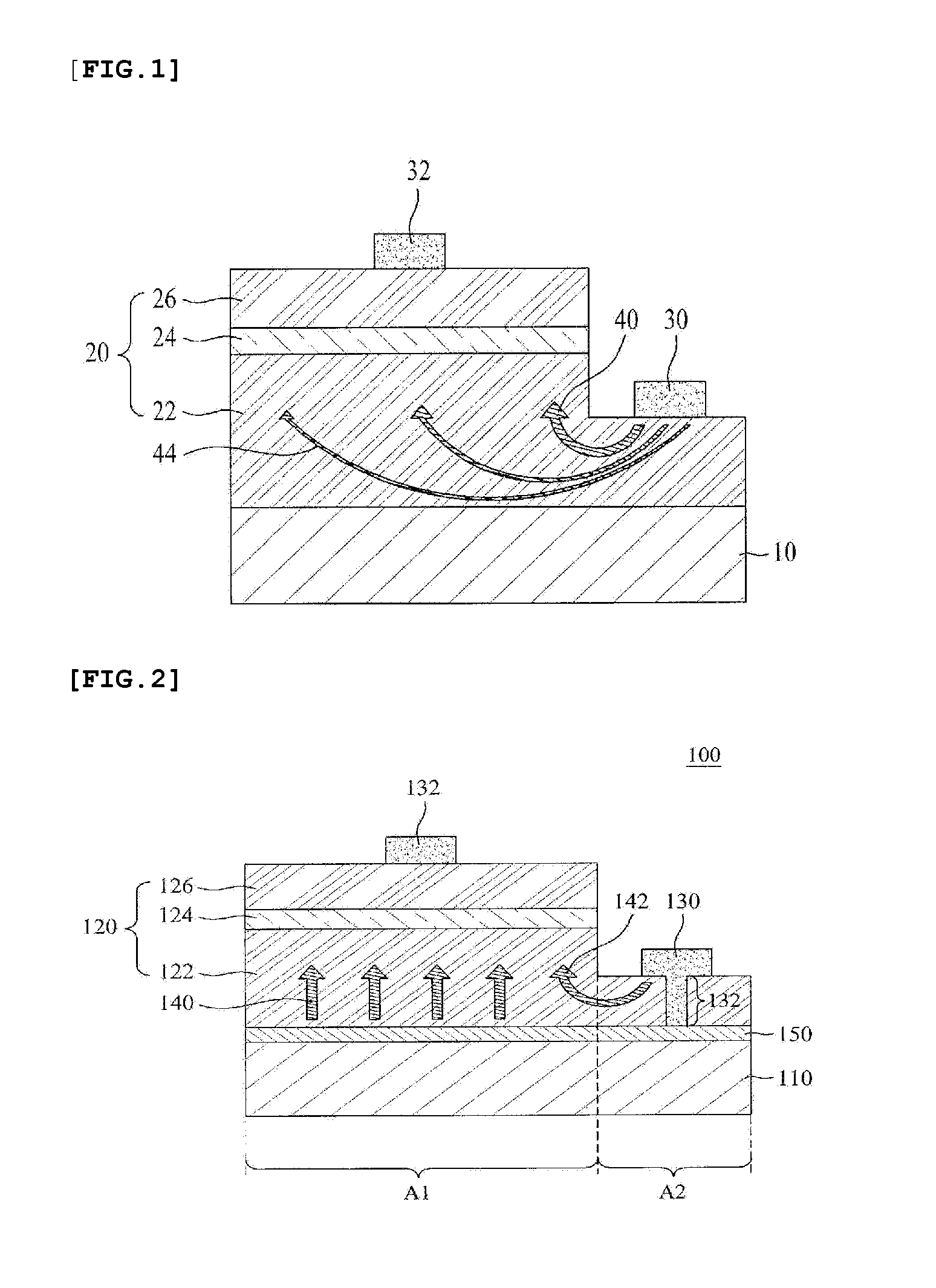
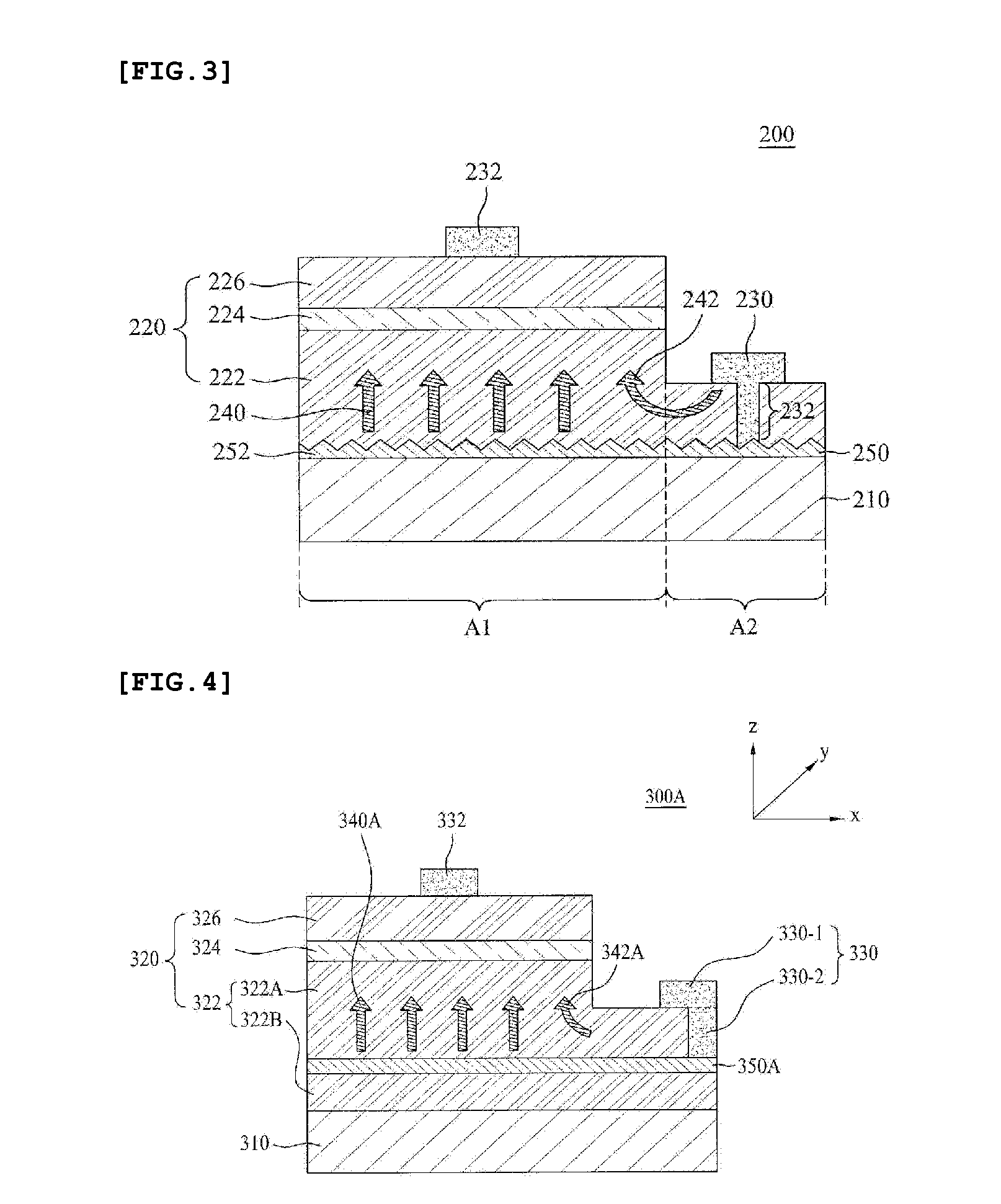
[0164]In a light emitting device according to embodiments, a conductive layer disposed between a light emitting layer and a substrate is electrically connected to a first electrode. As a result, the flow of carriers from the first electrode to an active layer is uniform. Consequently, it is possible to reduce driving voltage, to improve internal quantum efficiency, and to fundamentally prevent local heating of the light emitting device, thereby improving reliability of the light emitting device. In addition, the conductive layer is disposed in the middle of a first conductive semiconductor, i.e. between a first conductive lower semiconductor layer and a first conductive upper semiconductor layer. Consequently, it is possible to improve dislocation density.


PUM


Abstract

A light-emitting device, according to one embodiment, comprises a light-emitting structure having a silicon substrate, a first conductive type semiconductor layer disposed on the silicon substrate, an active layer, and a second conductive type semiconductor layer, a conductive layer facing the active layer between the silicon substrate and the first conductive type semiconductor layer, a first electrode which is disposed on the first conductive type semiconductor layer, penetrates or bypasses the first conductive type semiconductor layer, and is electrically connected to the conductive layer, and a second electrode disposed on the second conductive type semiconductor layer.

Description

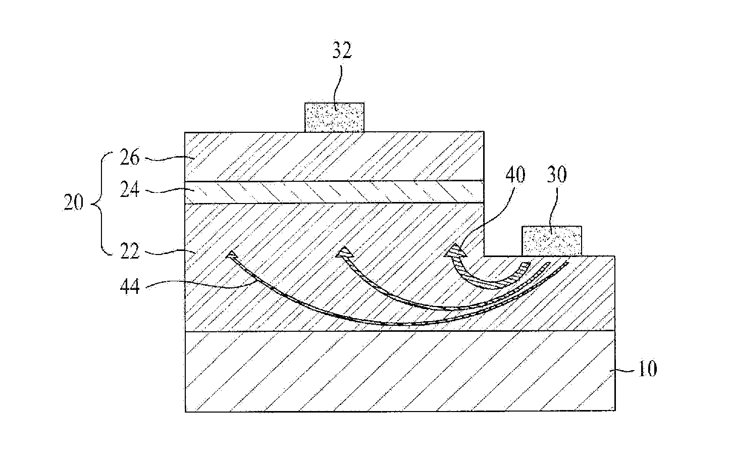
TECHNICAL FIELD[0001]Embodiments relate to a light emitting device.BACKGROUND ART[0002]A group III-V compound semiconductor, such as GaN, has been widely used in the field of optoelectronics since the semiconductor has wide and easily adjustable band gap energy and other advantages.[0003]FIG. 1 is a view showing a general horizontal-type light emitting device. Thicker arrows indicate flow of a larger number of electrons.[0004]The horizontal-type light emitting device shown in FIG. 1 includes a substrate 10 and a light emitting structure 20. The light emitting structure 20 includes an n-type semiconductor layer 22 disposed on the substrate 10, an active layer 24 disposed between the n-type semiconductor layer 22 and a p-type semiconductor layer 26, the p-type semiconductor layer 26 disposed on the active layer 24, and first and second electrodes 30 and 32 electrically contacting the n-type and p-type semiconductor layers 22 and 26, respectively.[0005]A larger portion of electrons sup...

Claims


Application Information

Patent Timeline
Patent Type & Authority Applications(United States)
IPC IPC(8): H01L33/14H01L33/04H01L33/10H01L33/30H01L33/36
CPCH01L33/14H01L33/30H01L33/04H01L33/10H01L33/36H01L33/20H01L33/38H01L33/382H01L33/385H01L2224/48091H01L33/0093H01L2924/00014H01L33/16
Inventor SONG, HYUN DONLEE, TAE LIMKIM, DONG HALEE, JIN WOOK
Owner LG INNOTEK CO LTD
Learn More