Method and system for smart card chip personalization

a technology of smart cards and personalization sequences, applied in the field of smart card chip personalization, can solve the problems of difficult reactivation with physical means, and the inability to replay personalization sequences

Inactive Publication Date: 2015-09-24
NAGRAVISION SA
View PDF0 Cites 15 Cited by
  • Summary
  • Abstract
  • Description
  • Claims
  • Application Information

AI Technical Summary

Problems solved by technology

a) Render personalization possible only at wafer level and extremely difficult to re-activate with physical means once the wafer is cut and the chip are packaged.
b) The personalization activation should not rely only on a single secret or on software package that can be owned (and leake

Method used


Image

  • Method and system for smart card chip personalization
  • Method and system for smart card chip personalization

Examples


Embodiment Construction

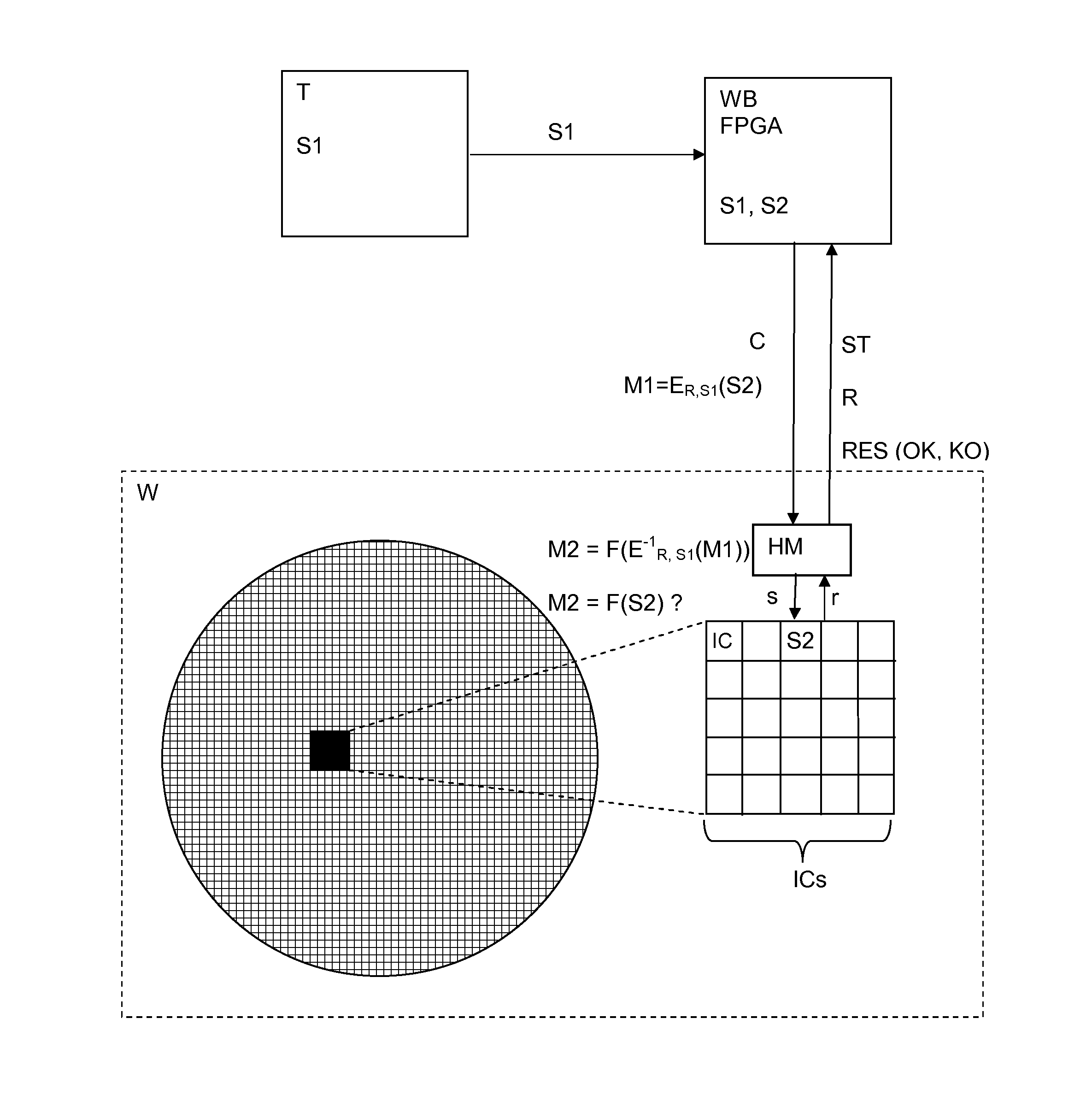
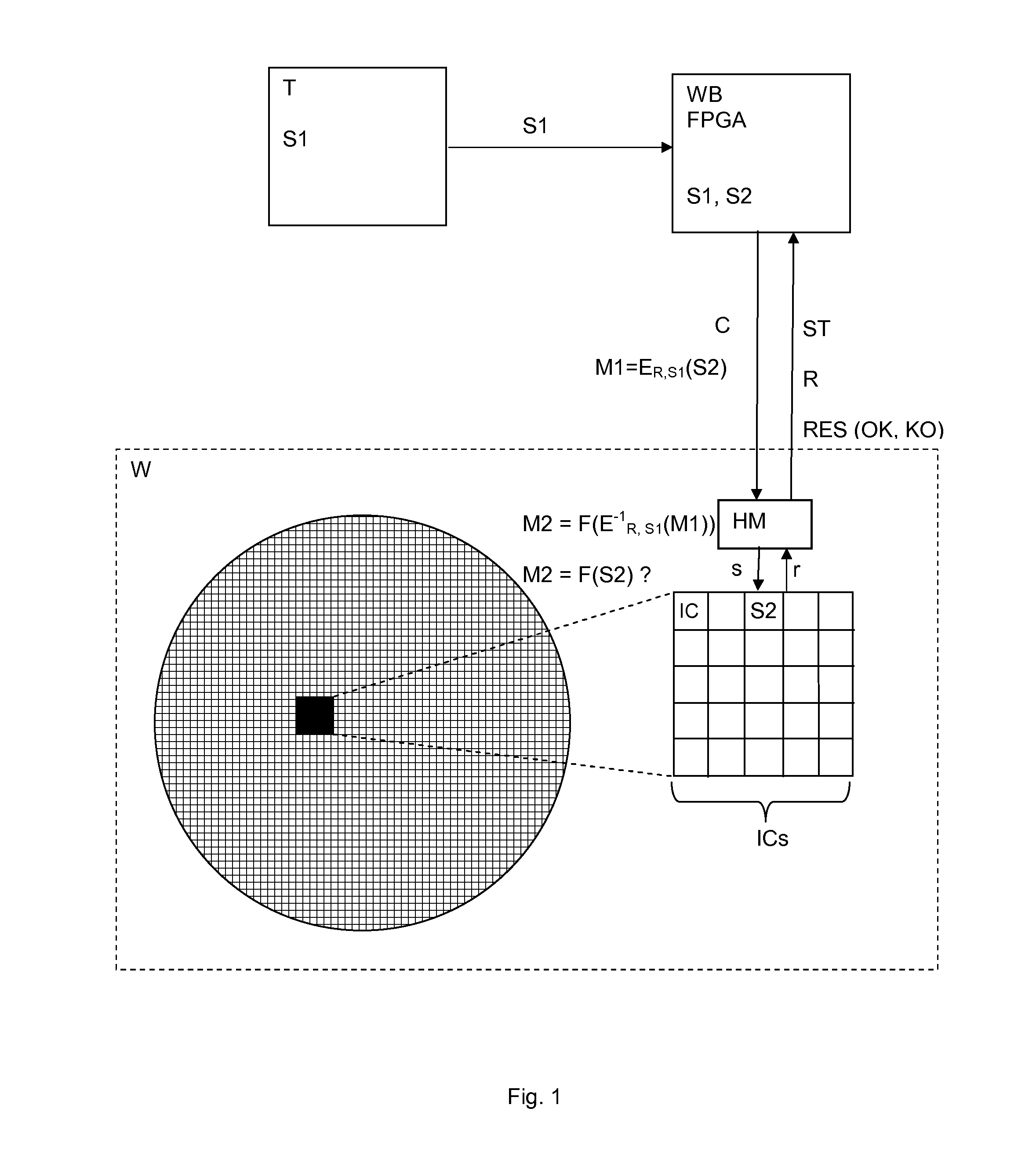
[0038]The system illustrated by FIG. 1 comprises a tester T associated to a FPGA device WB also called “waferbox” which configuration file is secured with known methods to prevent cloning. The test mode activation as well as the personalization process are preferably performed at wafer level i.e. the chips are arranged on a wafer used for their manufacturing. A hardware module HM preferably implemented on the wafer plays a role of interface between the FPGA device WB and the chips ICs on the wafer W and is in charge of verifying presence of the chip (s) ICs on the wafer W after initialization of the test mode. This verification prevents manipulations or attempt to modify personalization parameters when a chip is cut out of the wafer or integrated in a smart card in service in the field. The hardware module HM is destroyed at the end of personalization process during wafer cutting in order to separate all chips. Beside this physical security means, software and communication security...


PUM


Abstract

Method and system for personalizing a chip, intended to be integrated into a smart card, comprising a tester associated to an FPGA device connected to the chip, the chip being part of a wafer comprising a plurality of chips and a disposable hardware module for verifying presence of the chip on the wafer. The tester sends a first secret code to the FPGA device, which commands the chip to initiate a test mode activation. The FPGA device encrypts a second secret code by using a secret encryption algorithm parameterized with a random number received from the chip and the first secret code to obtain a first cryptogram which is sent to the chip. The chip determines a second cryptogram by carrying out a Boolean function over a result obtained by decryption of the first cryptogram using the inverse algorithm parameterized with the random number and the first secret code. The second cryptogram is compared with a result obtained by carrying out the Boolean function over the second secret code temporarily stored on the chip. The FPGA device personalizes the chip only if the second cryptogram matches the calculated result.

Description

FIELD OF THE INVENTION[0001]The invention relates to the domain of smart card chip personalization during which unique secrets and application code are embedded. In particular, the steps of personalization are performed under controlled conditions to prevent cloning and re-programming smart cards in the field.TECHNICAL BACKGROUND [0002]Secured chips are mostly used in manufacturing of smart cards, security modules, identification devices and other integrated circuits used in applications requiring a high security level.[0003]Document WO2010 / 130709A1 discloses a method for authenticating access to a secured chip by a test device. Once the test device is authenticated with the chip, i.e. successful verifications have been made by control data exchanges between the test device and the chip, the different operating tests or simulations are carried out on hardware and software functions and / or programs implemented in the chip. The test device can also comprise functionalities of configur...

Claims


Application Information

Patent Timeline
IPC IPC(8): H04L9/08H04L9/14
CPCH04L9/0869H04L2209/24H04L9/14G06F21/572G06F21/76G06F21/31G06F21/44H04L9/0643H04L9/0877H04L9/0897
Inventor HAUTIER, ROANMACCHETTI, MARCOPERRINE, JEROME
Owner NAGRAVISION SA
Why Eureka
Try Eureka