Eureka AIR delivers breakthrough ideas for toughest innovation challenges, trusted by R&D personnel around the world.

Semiconductor device having temperature sensor circuit that detects a temperature range upper limit value and a temperature range lower limit value

a technology of temperature sensor and semiconductor device, which is applied in the direction of heat measurement, pulse technique, instruments, etc., can solve the problems of increased leakage current, reduced drive current, and design problems

Active Publication Date: 2015-10-01
SAMSUNG ELECTRONICS CO LTD
View PDF11 Cites 16 Cited by
  • Summary
  • Abstract
  • Description
  • Claims
  • Application Information

AI Technical Summary

Benefits of technology

The present invention relates to a semiconductor device with temperature sensing circuits that provide operating parameter selection. The invention addresses the problem of unnecessary power consumption in semiconductor devices due to designing circuits for worst case temperatures. The invention provides a semiconductor device where parameters can be varied with respect to operating temperature, reducing power consumption at temperatures where the device operates. The invention includes a temperature sensing circuit that detects the temperature of the semiconductor device and adjusts the operating parameters accordingly. The invention also includes a power up circuit that adjusts the power supply voltage based on the detected temperature. The invention provides a semiconductor device with improved battery life and reduced power consumption for mobile devices.

Problems solved by technology

Although drive current decreases, leakage current (leakage current when the IGFET is turned off) increases.
These temperature dependent characteristics can make design problematic.
By designing circuits in a semiconductor device for a worst case temperature, power may be unnecessarily wasted at another temperature point.
For example, a power supply may provide a voltage that is unnecessarily high at a first temperature point due to the necessity of ensuring specifications are met at a second temperature point, even though the semiconductor device rarely operates at the second temperature point.
This can cause power to be wasted at the first temperature point, which is where the semiconductor device typically operates.
However, to ensure specifications are met, the frequency of refresh operations may be unnecessarily high at low temperatures to ensure the high temperature case is met.
This can cause unnecessary power consumption in typical operating temperatures.
Unnecessary power consumption is even more important in mobile devices as it reduces battery lifetime.

Method used


Image

  • Semiconductor device having temperature sensor circuit that detects a temperature range upper limit value and a temperature range lower limit value
  • Semiconductor device having temperature sensor circuit that detects a temperature range upper limit value and a temperature range lower limit value
  • Semiconductor device having temperature sensor circuit that detects a temperature range upper limit value and a temperature range lower limit value

Examples


Embodiment Construction

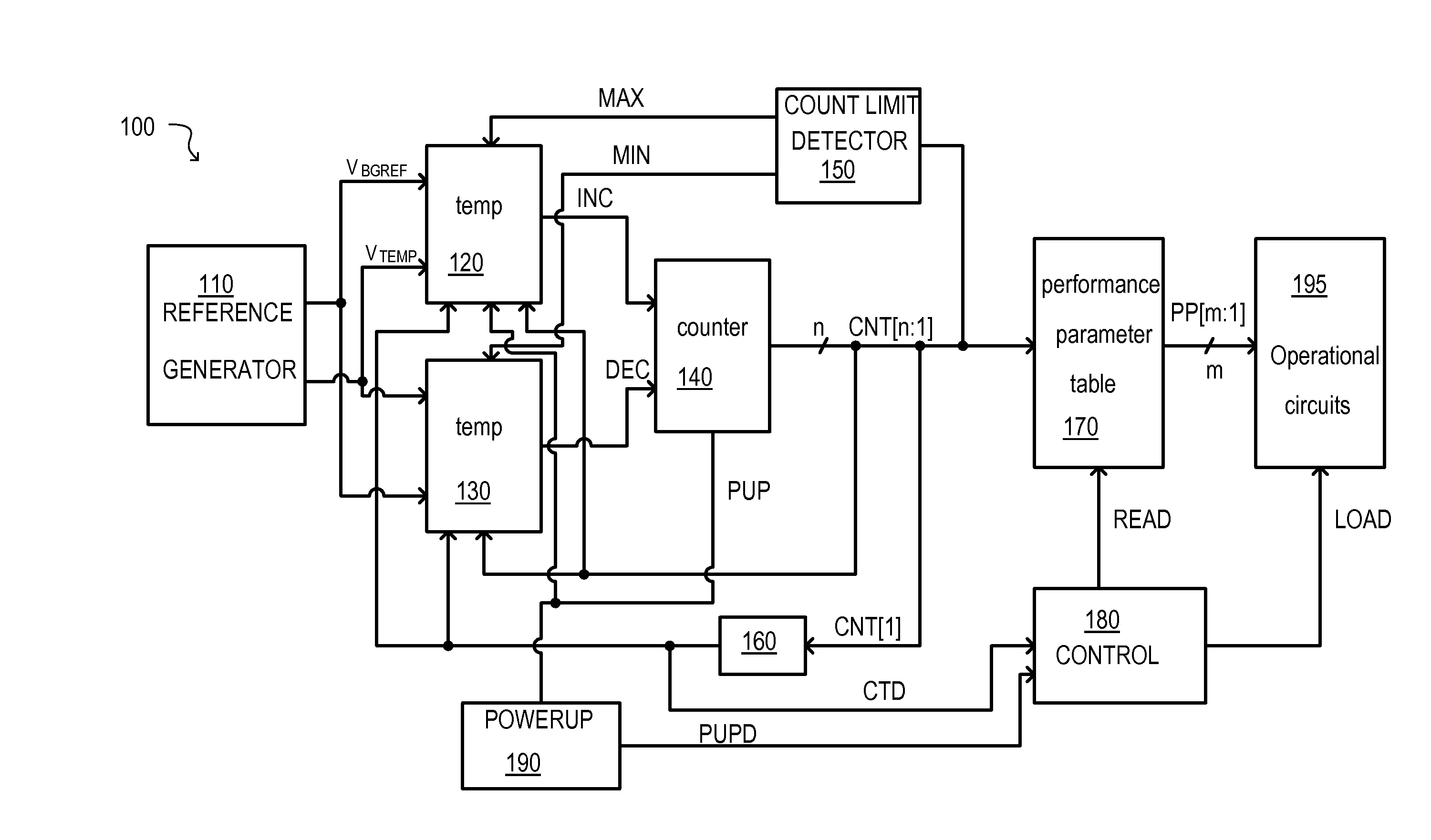
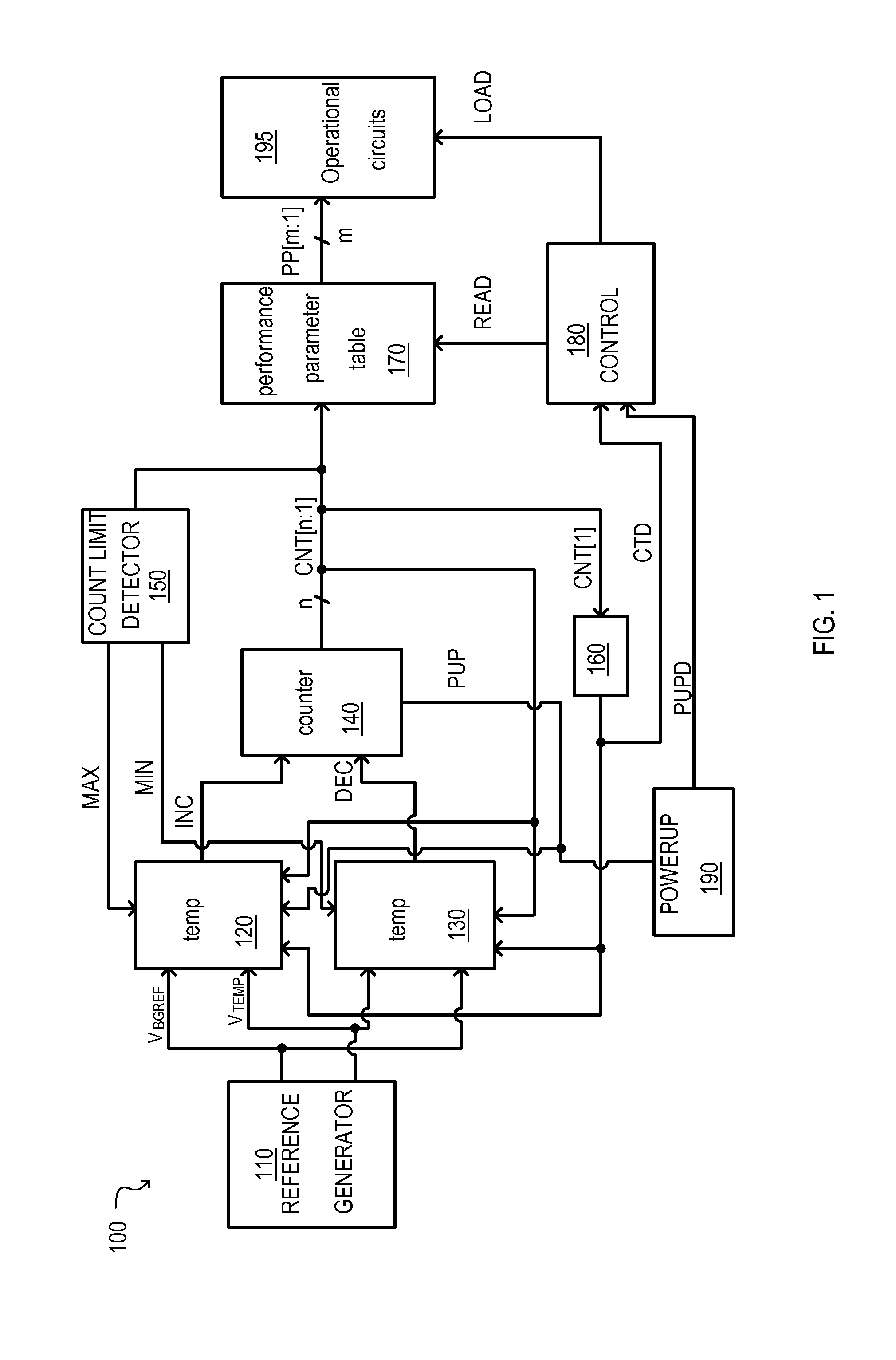
[0035]According to the embodiments set forth below, a semiconductor device can include a temperature sensing circuit. The temperature sensing circuits can include at least one variable resistor that can set a temperature range. A counter may incrementally change in accordance with a temperature of the semiconductor device changing outside of the bounds of the range. The resistance value of the at least one variable resistor can change in response to the count output of the counter such that the temperature range can change. Furthermore, the value of the counter may select parameters stored in a table to set performance parameters of various operational circuits. In this way, functionality of the semiconductor device may be assured over a large temperature range without wasting power and / or degrading performance unnecessarily.

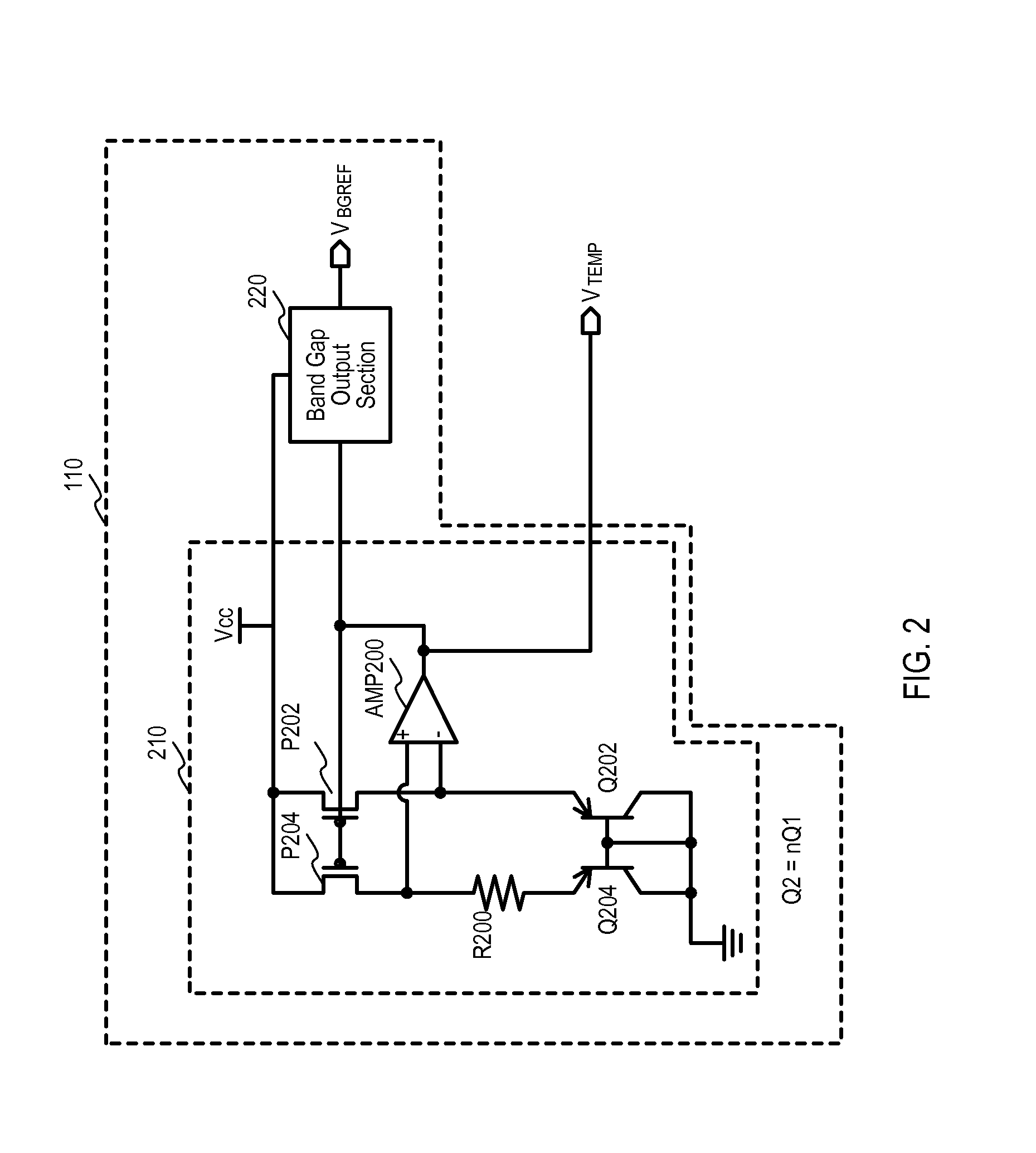
[0036]Referring now to FIG. 1, a semiconductor device according to an embodiment is set forth in a block schematic diagram and given the general reference chara...


PUM


Abstract

A semiconductor device that may include at least one temperature sensing circuit is disclosed. The temperature sensing circuits may be used to control various operating parameters to improve the operation of the semiconductor device over a wide temperature range. In this way, operating specifications of a semiconductor device at worst case temperatures may be met without compromising performance at other operating temperatures. The temperature sensing circuit may provide a plurality of temperature ranges for setting the operational parameters. Each temperature range can include a temperature range upper limit value and a temperature range lower limit value and adjacent temperature ranges may overlap. The temperature ranges may be set in accordance with a count value that can incrementally change in response to the at least one temperature sensing circuit.

Description

[0001]This application claims the benefit of U.S. Provisional Patent Application Ser. No. 61 / 971,702, filed Mar. 28, 2014, the contents of which are incorporated by reference herein.TECHNICAL FIELD[0002]The present invention relates generally to a semiconductor device, and more particularly to a semiconductor device including temperature sensing circuits that provide operating parameter selection.BACKGROUND OF THE INVENTION[0003]Semiconductor devices include components that have characteristics that vary with respect to temperature. For example, as temperature increases mobility of charge carriers decrease causing transistors, such as insulated gate field effect transistors (IGFET) to have lower drive current. Although drive current decreases, leakage current (leakage current when the IGFET is turned off) increases. These temperature dependent characteristics can make design problematic.[0004]When designing a semiconductor device, the designer will design circuit timing and internal...

Claims


Application Information

Patent Timeline
IPC IPC(8): G01K7/16G11C7/00
CPCG11C7/00G01K7/16G01K3/005G01K7/01G11C7/04G11C11/40626H03K17/145H03K17/223H03K21/10G01K7/00G01K13/00G11C11/407G11C11/4074G11C11/4093G11C11/4096H03K3/012H03K17/687
Inventor WALKER, DARRYL G.
Owner SAMSUNG ELECTRONICS CO LTD
Why Eureka
Eureka Blog
Learn More