Eureka AIR delivers breakthrough ideas for toughest innovation challenges, trusted by R&D personnel around the world.

System and Method for Integrated Circuit Manufacturing

a technology of integrated circuits and manufacturing methods, applied in the field of integrated circuit manufacturing systems and methods, can solve the problems of preventing the device from performing as desired, inaccurate or poorly shaped device features, and increasing the complexity of processing and manufacturing ics

Active Publication Date: 2015-10-01
TAIWAN SEMICON MFG CO LTD
View PDF5 Cites 463 Cited by
  • Summary
  • Abstract
  • Description
  • Claims
  • Application Information

AI Technical Summary

Benefits of technology

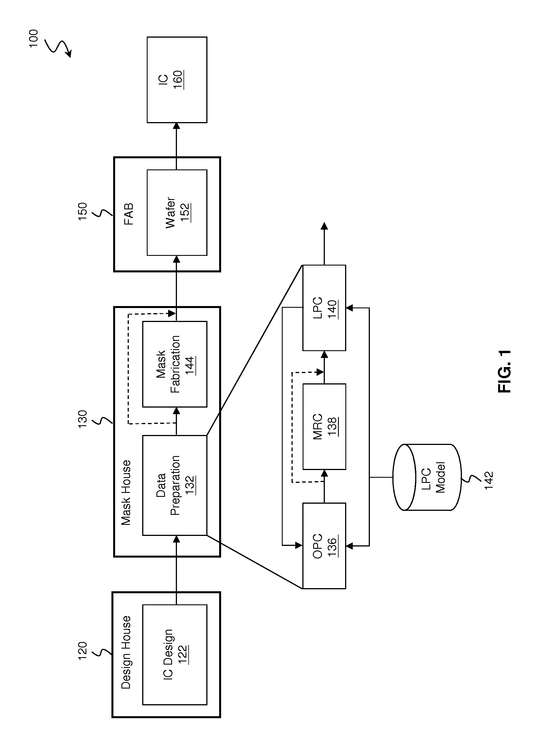
The patent text describes a method for improving the manufacturing of integrated circuits (ICs) by using optical proximity correction (OPC) to correct the shapes of design patterns and create assist features to improve device performance. The technical effect of this method is to improve the accuracy and performance of ICs by addressing issues such as rounded corners, pinching, and metal line thickness variations. The patent text also describes the various components and processes involved in the IC manufacturing process, including design house, mask house, and IC manufacturer.

Problems solved by technology

Such scaling down has also increased the complexity of processing and manufacturing ICs and, for these advances to be realized, similar developments in IC manufacturing are needed.
As IC technologies are continually progressing to smaller technology nodes, simply scaling down similar designs used at larger nodes often results in inaccurate or poorly shaped device features.
For example, rounded corners on a device feature that is designed to have right-angle corners may become more pronounced or more critical in the smaller nodes, preventing the device from performing as desired.

Method used


Image

  • System and Method for Integrated Circuit Manufacturing
  • System and Method for Integrated Circuit Manufacturing
  • System and Method for Integrated Circuit Manufacturing

Examples


Embodiment Construction

[0010]It is to be understood that the following disclosure provides many different embodiments, or examples, for implementing different features of the disclosure. Specific examples of components and arrangements are described below to simplify the present disclosure. These are, of course, merely examples and are not intended to be limiting. In addition, the present disclosure may repeat reference numerals and / or letters in the various examples. This repetition is for the purpose of simplicity and clarity and does not in itself dictate a relationship between the various embodiments and / or configurations discussed. Moreover, the performance of a first process before a second process in the description that follows may include embodiments in which the second process is performed immediately after the first process, and may also include embodiments in which additional processes may be performed between the first and second processes. Various features may be arbitrarily drawn in differe...


PUM


Abstract

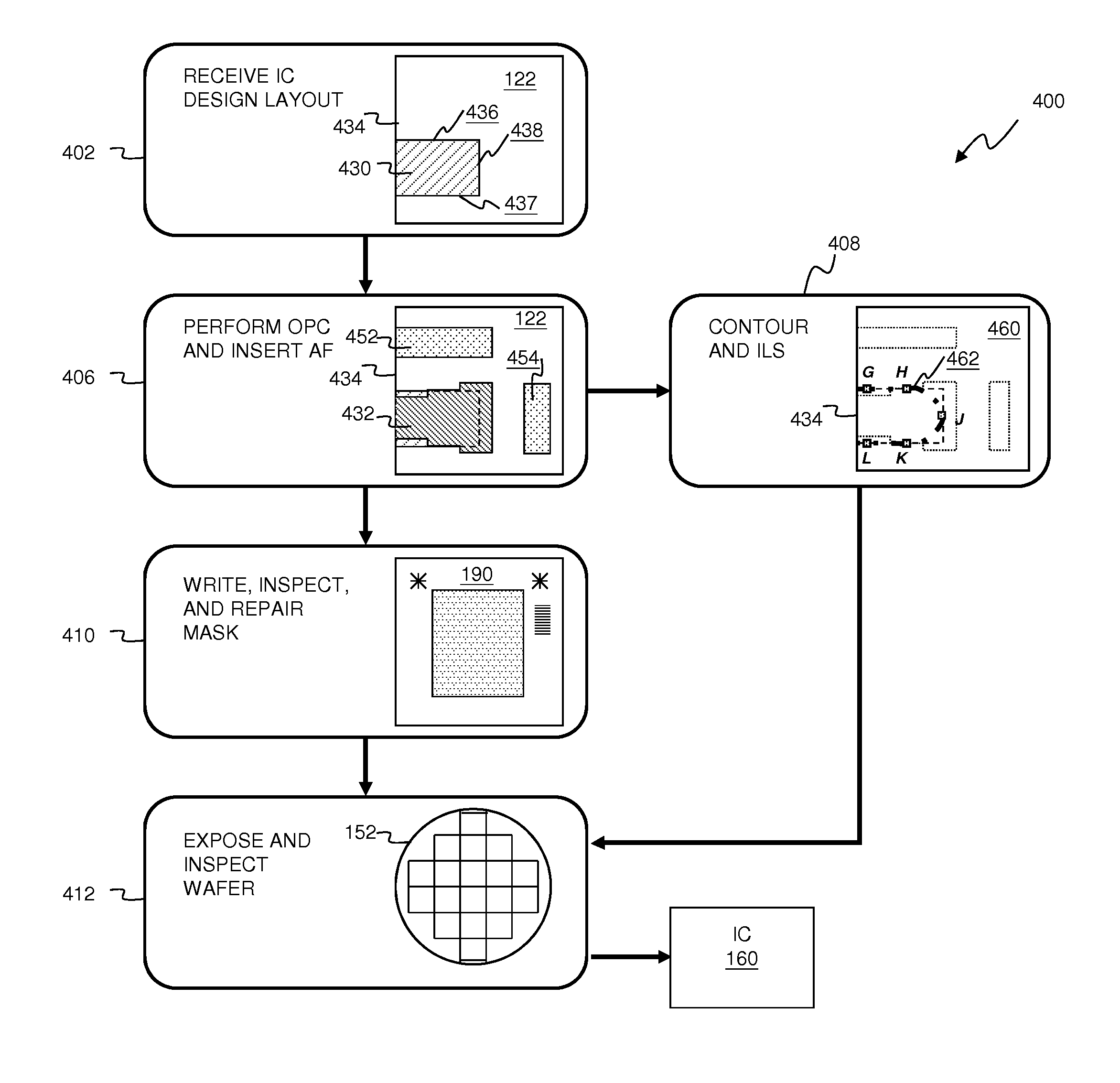
Provided is an integrated circuit (IC) manufacturing method. The method includes receiving a design layout of an IC, the design layout having a main feature; performing a process correction to the main feature thereby generating a modified main feature; using a computer, generating a simulated contour of the modified main feature, the simulated contour having a plurality of points; generating a plurality of assistant data in computer readable format, wherein each assistant data includes at least one process performance factor associated with one of the points; and keeping the simulated contour and the assistant data for use by a further process stage, such as mask making, mask inspection, mask repairing, wafer direct writing, wafer inspection, and wafer repairing.

Description

BACKGROUND[0001]The semiconductor integrated circuit (IC) industry has experienced rapid growth. In the course of IC evolution, functional density (i.e., the number of interconnected devices per chip area) has generally increased while geometry size (i.e., the smallest component (or line) that can be created using a fabrication process) has decreased. This scaling down process generally provides benefits by increasing production efficiency and lowering associated costs. Such scaling down has also increased the complexity of processing and manufacturing ICs and, for these advances to be realized, similar developments in IC manufacturing are needed.[0002]As IC technologies are continually progressing to smaller technology nodes, simply scaling down similar designs used at larger nodes often results in inaccurate or poorly shaped device features. For example, rounded corners on a device feature that is designed to have right-angle corners may become more pronounced or more critical in ...

Claims


Application Information

Patent Timeline
IPC IPC(8): G06F17/50
CPCG06F17/5009G06F17/5081G03F7/70441G06F30/398G06F2119/18Y02P90/02G03F1/36
Inventor CHANG, SHIH-MING
Owner TAIWAN SEMICON MFG CO LTD
Why Eureka
Eureka Blog
Learn More