
Display device

Inactive Publication Date: 2015-10-15
SAMSUNG DISPLAY CO LTD
View PDF1 Cites 0 Cited by
  • Summary
  • Abstract
  • Description
  • Claims
  • Application Information

AI Technical Summary

Benefits of technology

The present invention provides a display device that has advantages of being lightweight, thin, cost-effective, and processing time-efficient. This is achieved by manufacturing the display device using no more than one substrate. Additionally, the invention also prevents cross talk that occurs due to high resistance of a common electrode. The common electrode is connected with a storage electrode line, which reduces its resistance.

Problems solved by technology

However, in a liquid crystal display in the related art, two sheets of substrates are necessarily used, and respective constituent elements are formed on the two sheets of substrates, and as a result, there are problems in that the display device is heavy and thick, has high cost, and has a long processing time.

Method used


Image

  • Display device
  • Display device
  • Display device

Examples


Embodiment Construction

[0034]The inventive concept will be described more fully hereinafter with reference to the accompanying drawings, in which exemplary embodiments are shown. As those skilled in the art would realize, the described embodiments may be modified in various different ways, all without departing from the spirit or scope of the inventive concept.

[0035]In the drawings, the thickness of layers, films, panels, regions, etc., are exaggerated for clarity. Like reference numerals designate like elements throughout the specification. It will be understood that when an element such as a layer, film, region, or substrate is referred to as being “on” another element, it can be directly on the other element or intervening elements may also be present. In contrast, when an element is referred to as being “directly on” another element, there are no intervening elements present.

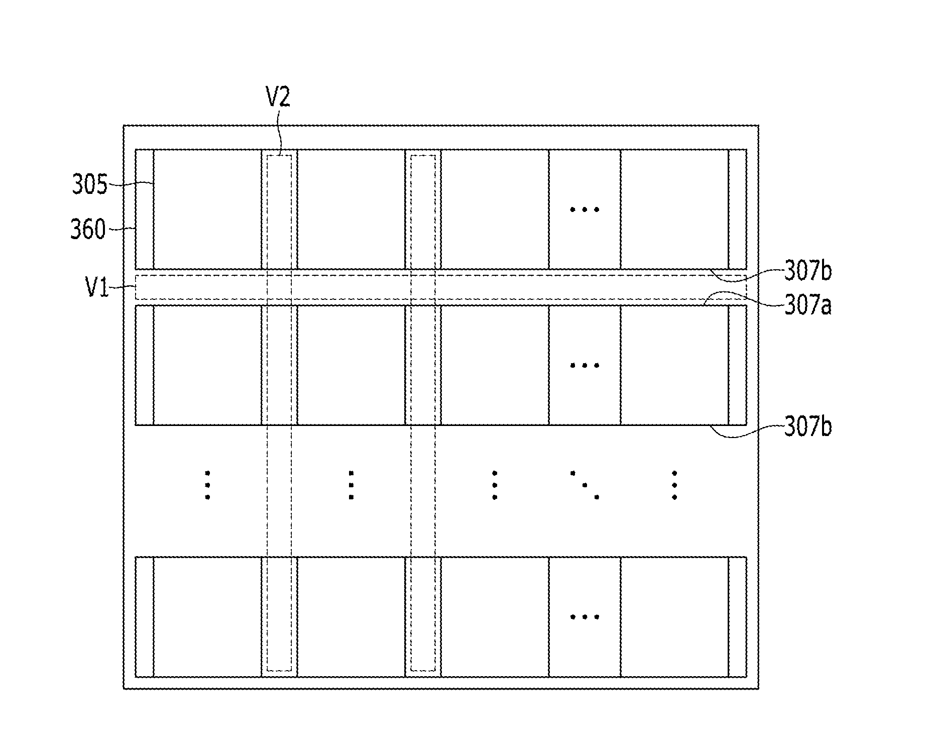
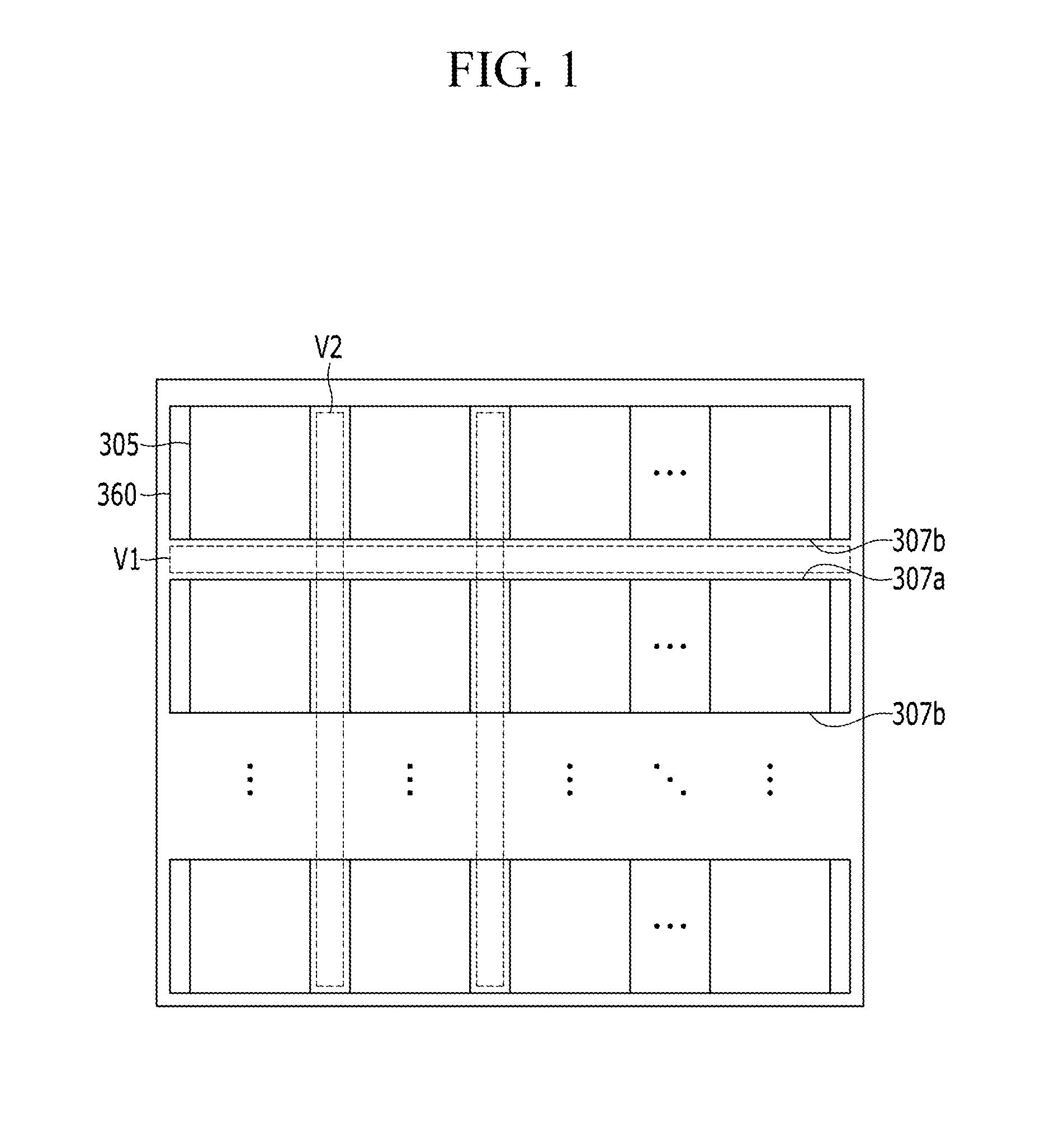
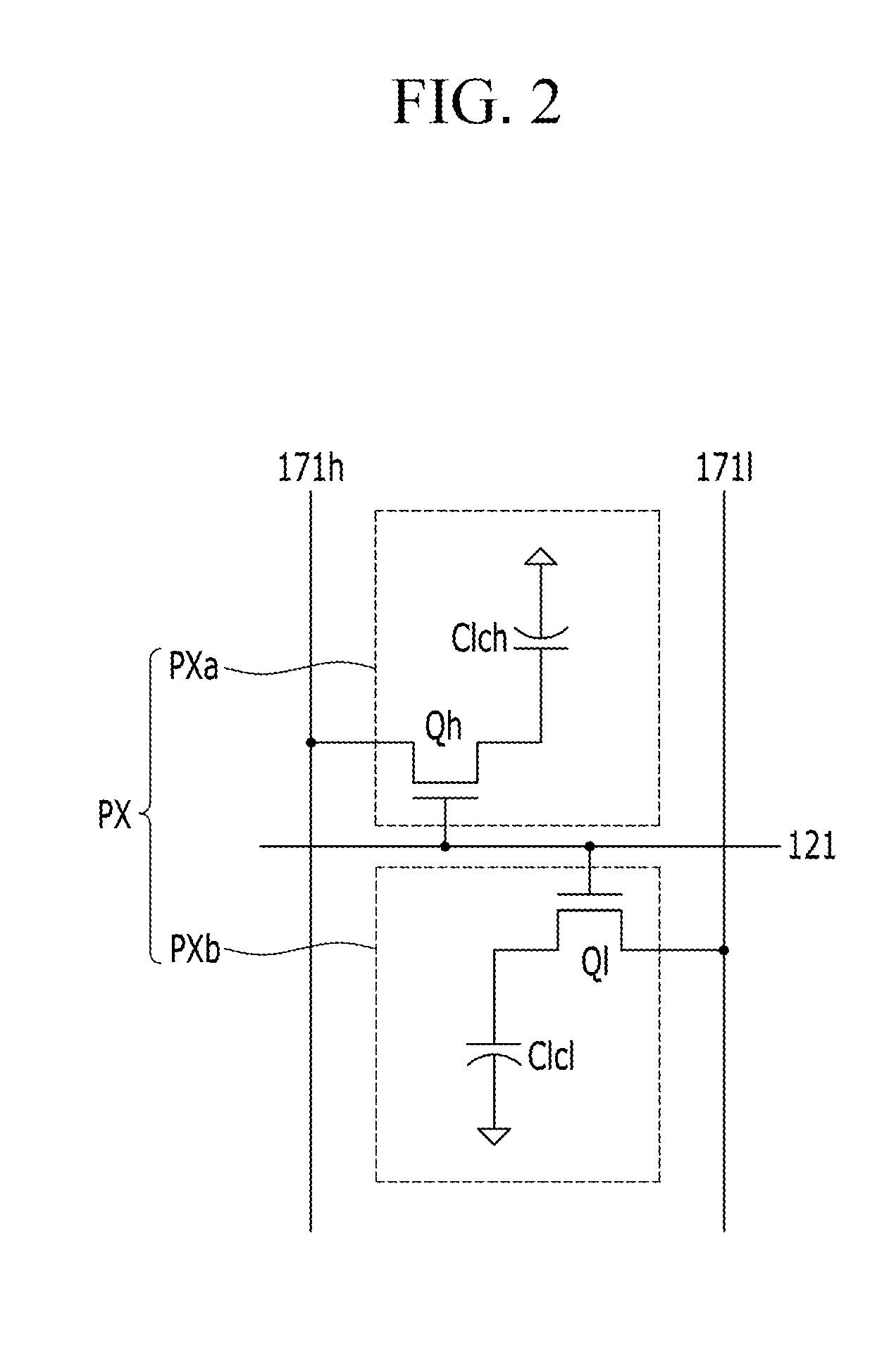
[0036]First, a display device according to an exemplary embodiment of the inventive concept will be schematically described belo...


PUM

PropertyMeasurementUnit
Shapeaaaaaaaaaa
Electric potential / voltageaaaaaaaaaa

Abstract

A display device capable of reducing a resistance of a common electrode is presented. The display device includes: a substrate; a gate line, a data line, and a storage electrode line formed on the substrate; a thin film transistor connected to the gate line and the data line; a pixel electrode connected with the thin film transistor; a common electrode formed on the pixel electrode ; a plurality of microcavities between the common electrode and the pixel electrode; a roof layer formed on the common electrode; a liquid crystal layer in the microcavity; and an encapsulation layer formed on the roof layer to seal the microcavity, wherein the common electrode is connected with the storage electrode line at a position adjacent to the data line.

Description

CROSS-REFERENCE TO RELATED APPLICATION[0001]This application claims priority to and the benefit of Korean Patent Application No. 10-2014-0044981 filed in the Korean Intellectual Property Office on Apr. 15, 2014, the entire contents of which are incorporated herein by reference.BACKGROUND[0002](a) Technical Field[0003]The present invention relates to a display device, and more particularly, to a display device capable of reducing common electrode resistance.[0004](b) Description of the Related Art[0005]A liquid crystal display, which is one of the most common types of flat panel displays currently in use, includes two sheets of display panels with field generating electrodes such as a pixel electrode, a common electrode, and the like, and a liquid crystal layer interposed therebetween. The liquid crystal display generates an electric field in the liquid crystal layer by applying a voltage to the field generating electrodes to determine alignment of liquid crystal molecules through th...

Claims


Application Information

Patent Timeline
IPC IPC(8): G02F1/1343G02F1/133G02F1/1333G02F1/1362G02F1/1368
CPCG02F1/134336G02F1/136286G02F1/13306G02F1/133345G02F1/1368G02F1/133377G02F1/133707G02F1/13624G02F1/134345G02F1/1334
Inventor CHAE, KYUNG TAEKIM, WON TAELEE, SUN HWA
Owner SAMSUNG DISPLAY CO LTD
Features
  • Generate Ideas
  • Intellectual Property
  • Life Sciences
  • Materials
  • Tech Scout
  • Unparalleled Data Quality
  • Higher Quality Content
  • 60% Fewer Hallucinations
Learn More