Supercharge Your Innovation With Domain-Expert AI Agents!

Semiconductor interposer and package structure having the same

a technology of semiconductors and interposers, applied in the direction of semiconductor devices, solid-state devices, basic electric elements, etc., can solve the problems of reducing product reliability, reducing product reliability, and failure of reliability tests, so as to reduce stress and reduce stress , the effect of small stress

Active Publication Date: 2015-10-22
SILICONWARE PRECISION IND CO LTD
View PDF4 Cites 2 Cited by
  • Summary
  • Abstract
  • Description
  • Claims
  • Application Information

AI Technical Summary

Benefits of technology

The present invention is about a method to prevent warping of a semiconductor interposer and to avoid delamination of the UBM layer or cracking of a conductive element on the UBM layer. This is achieved by creating a passivation layer with different portions that experience different stresses. The peripheral portion is formed in the peripheral area of the semiconductor interposer that usually experiences large stresses, while the ring-shaped and strip-shaped portions are formed in the inner area that usually experiences small stresses. This results in effective reduction of stresses and prevents warping of the semiconductor interposer.

Problems solved by technology

In a flip-chip packaging process, a big CTE (Coefficient of Thermal Expansion) mismatch between a chip and a packaging substrate adversely affects the formation of joints between conductive bumps of the chip and contacts of the packaging substrate, thus easily resulting in delamination of the conductive bumps from the packaging substrate.
On the other hand, along with increased integration of integrated circuits, the CIE mismatch between the chip and the packaging substrate induces more thermal stresses and leads to more serious warpage, thereby reducing the product reliability and resulting in failure of a reliability test.
However, such a small thickness easily leads to warping of the silicon interposer 12 during fabrication of the silicon interposer 12, when the semiconductor chips 11 are disposed on the silicon interposer 12 or when the silicon interposer 12 is disposed on the packaging substrate 13, thereby generating large stresses on conductive elements 14 (such as u-bumps) between the semiconductor chips 11 and the silicon interposer 12 or conductive elements 15 (such as c4 bumps) between the silicon interposer 12 and the packaging substrate 13 and hence easily causing cracking of the joints.
Particularly, serious cracking often occurs to the conductive elements 14.
In addition, when processes such as chip mounting processes or heating processes are performed after singulation of the silicon interposer 12, large stresses easily occur around a periphery of the silicon interposer 12, which easily cause warping of the silicon interposer 12 and consequently reduce the reliability of final products.

Method used


Image

  • Semiconductor interposer and package structure having the same
  • Semiconductor interposer and package structure having the same
  • Semiconductor interposer and package structure having the same

Examples


Embodiment Construction

[0026]The following illustrative embodiments are provided to illustrate the disclosure of the present invention, these and other advantages and effects can be apparent to those in the art after reading this specification.

[0027]It should be noted that all the drawings are not intended to limit the present invention.

[0028]Various modifications and variations can be made without departing from the spirit of the present invention. Further, terms such as “on”, “a” etc. are merely for illustrative purposes and should not be construed to limit the scope of the present invention.

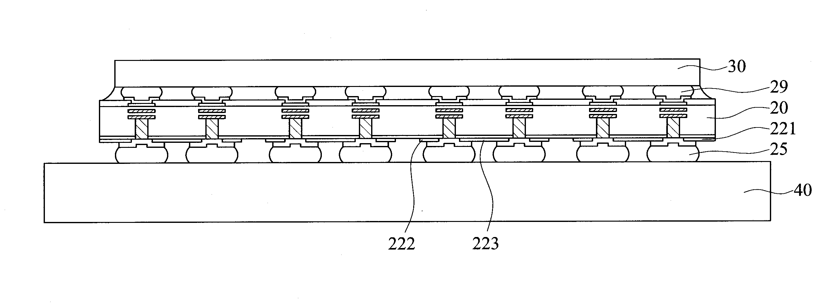
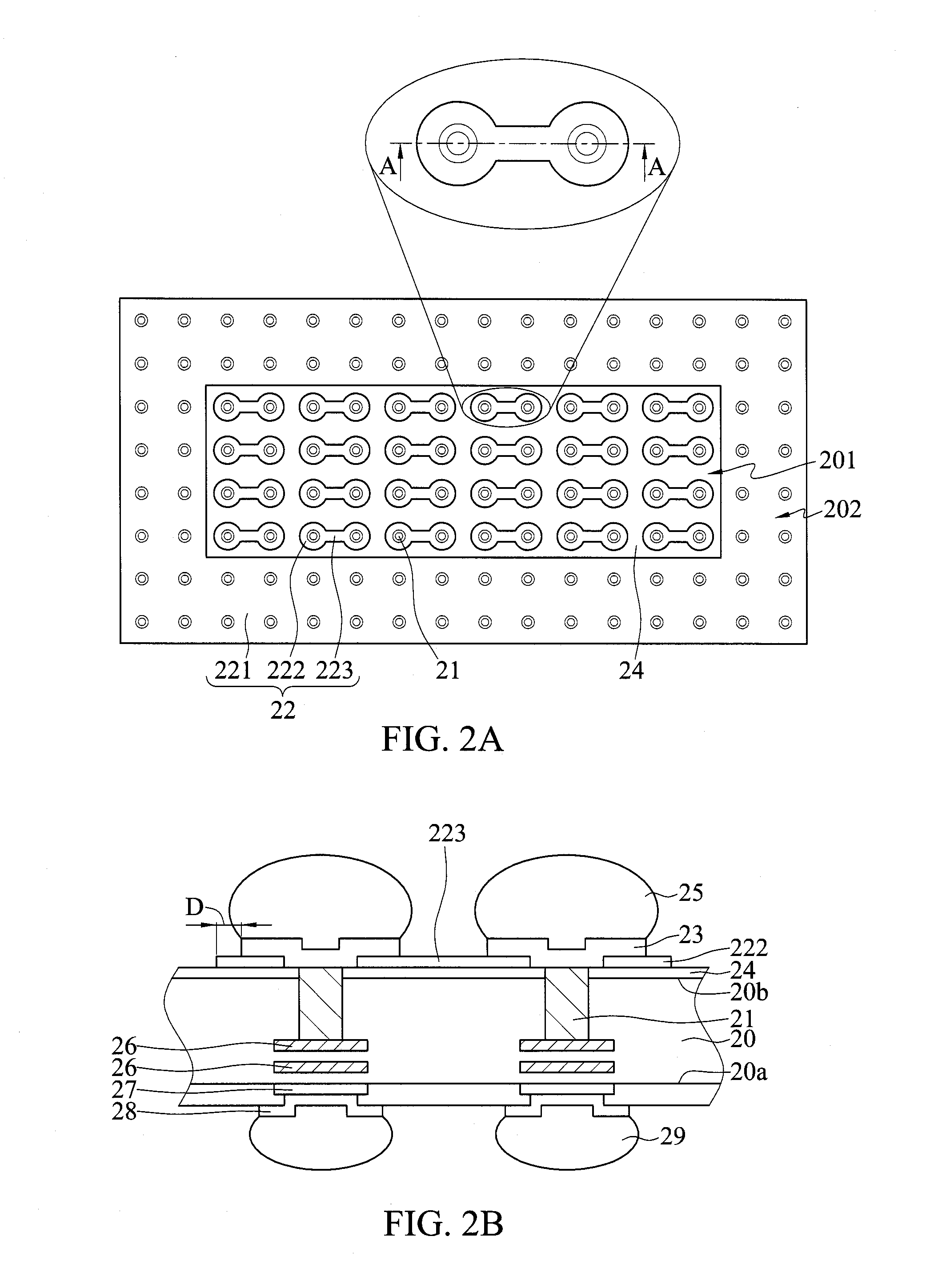
[0029]FIG. 2A is a schematic top view of a semiconductor interposer of the present invention, and FIG. 2B is a partially cross-sectional view of the semiconductor interposer along a sectional line AA of FIG. 2A. Referring to FIGS. 2A and 2B, the semiconductor interposer of the present invention has a substrate body 20 having opposite first and second surfaces 20a, 20b. The second surface 20b of the substrate body 20...


PUM


Abstract

A semiconductor interposer is provided, which includes: a substrate body having a surface defined with an inner area and a peripheral area around the inner area; a plurality of conductive posts embedded in the substrate body and each having one end exposed from the surface of the substrate body; a passivation layer formed on the surface of the substrate body and having a peripheral portion formed in the peripheral area, a plurality of ring-shaped portions formed around peripheries of the exposed ends of the conductive posts in the inner area and a plurality of strip-shaped portions formed between the ring-shaped portions for connecting the ring-shaped portions; and a UBM layer formed on the exposed end of each of the conductive posts and extending on the ring-shaped portion around the periphery of the exposed end of the conductive post, thereby effectively reducing stresses to prevent warping of the semiconductor interposer.

Description

BACKGROUND OF THE INVENTION[0001]1. Field of the Invention[0002]The present invention relates to semiconductor interposers and package structures having the same, and more particularly, to a semiconductor interposer having a UBM (Under Bump Metallurgy) layer and a package structure having the semiconductor interposer.[0003]2. Description of Related Art[0004]Flip-chip technologies facilitate to reduce chip packaging sizes and shorten signal transmission paths and therefore have been widely used for chip packaging. Various types of packages such as chip scale packages (CSPs), direct chip attached (DCA) packages and multi-chip module (MCM) packages can be achieved through flip-chip technologies.[0005]In a flip-chip packaging process, a big CTE (Coefficient of Thermal Expansion) mismatch between a chip and a packaging substrate adversely affects the formation of joints between conductive bumps of the chip and contacts of the packaging substrate, thus easily resulting in delamination of ...

Claims


Application Information

Patent Timeline
IPC IPC(8): H01L23/498H01L23/31H01L23/00
CPCH01L23/49838H01L23/49811H01L2224/16227H01L23/3171H01L2224/16113H01L24/17H01L23/147H01L23/49827H01L2224/16235
Inventor TSAI, JYUN-LINGLU, CHANG-LUN
Owner SILICONWARE PRECISION IND CO LTD
Features
  • R&D
  • Intellectual Property
  • Life Sciences
  • Materials
  • Tech Scout
  • Unparalleled Data Quality
  • Higher Quality Content
  • 60% Fewer Hallucinations
Learn More