Nanowire electric field effect sensor having three-dimensional stacking structure nanowire and manufacturing method therefor

a nanowire and electric field effect technology, which is applied in the field of nanowire field effect sensors comprising nanowires, can solve the problems of increasing difficulty, decreasing the number of elements per substrate area, and difficulty in maintaining the difference in properties between the nanowires at a constant level, so as to increase the probability of attachment of a target material to the nanowires of the sensor of the present invention, the effect of increasing the sensing area and increasing the sensitivity

Active Publication Date: 2015-10-22
POSTECH ACAD IND FOUND
View PDF3 Cites 11 Cited by
  • Summary
  • Abstract
  • Description
  • Claims
  • Application Information

AI Technical Summary

Benefits of technology

[0013]The nanowire sensor comprising nanowires having a three-dimensional stacked structure according to the present invention has a larger sensing area compared to a conventional nanowire sensor having a two-dimensional nanowire structure in the same limited area. Thus, the probability of attachment of a target material to the nanowires of the sensor of the present invention can be increased, and the change in electrical conductivity (conductance or resistance) by the attached target material can be sensed with higher sensitivity, suggesting that the sensor has increased sensitivity.
[0014]In addition, a medium is filled in the upper, side and lower portions of the nanowire layer, and thus the element is operated like GAA (gate-all-around) FETs. Thus, the ability of the nanowires to control the gate is increased to the increase the sensitivity of the sensor.
[0015]The term “GAA (gate-all-around)” means that all the four sides of the nanowire layer are used as a gate electrode 31, and the detailed description thereof is omitted herein, because it is obvious to those skilled in the art.
[0016]In addition, due to the influence of the nanowires disposed in parallel, a nanowire having high electrical conductivity influences the entire element. Accordingly, the on-state characteristics of the element are influenced mainly by a nanowire having excellent performance among the nanowires connected in parallel so that the average on-state characteristics of the element will be improved.

Problems solved by technology

However, because the nanowire channel is a one-dimensional structure, it is sensitively influenced by traps present in the nanowire and a gate insulating layer covering the nanowire, and thus it is difficult to maintain the difference in properties between the nanowires at a constant level, and this difficulty becomes more severe as the length of the nanowires increases.
This causes a problem in that the number of elements per substrate area decreases.

Method used


Image

  • Nanowire electric field effect sensor having three-dimensional stacking structure nanowire and manufacturing method therefor
  • Nanowire electric field effect sensor having three-dimensional stacking structure nanowire and manufacturing method therefor
  • Nanowire electric field effect sensor having three-dimensional stacking structure nanowire and manufacturing method therefor

Examples


Embodiment Construction

[0030]Hereinafter, exemplary embodiments of the present invention will be described in detail with reference to the accompanying drawings.

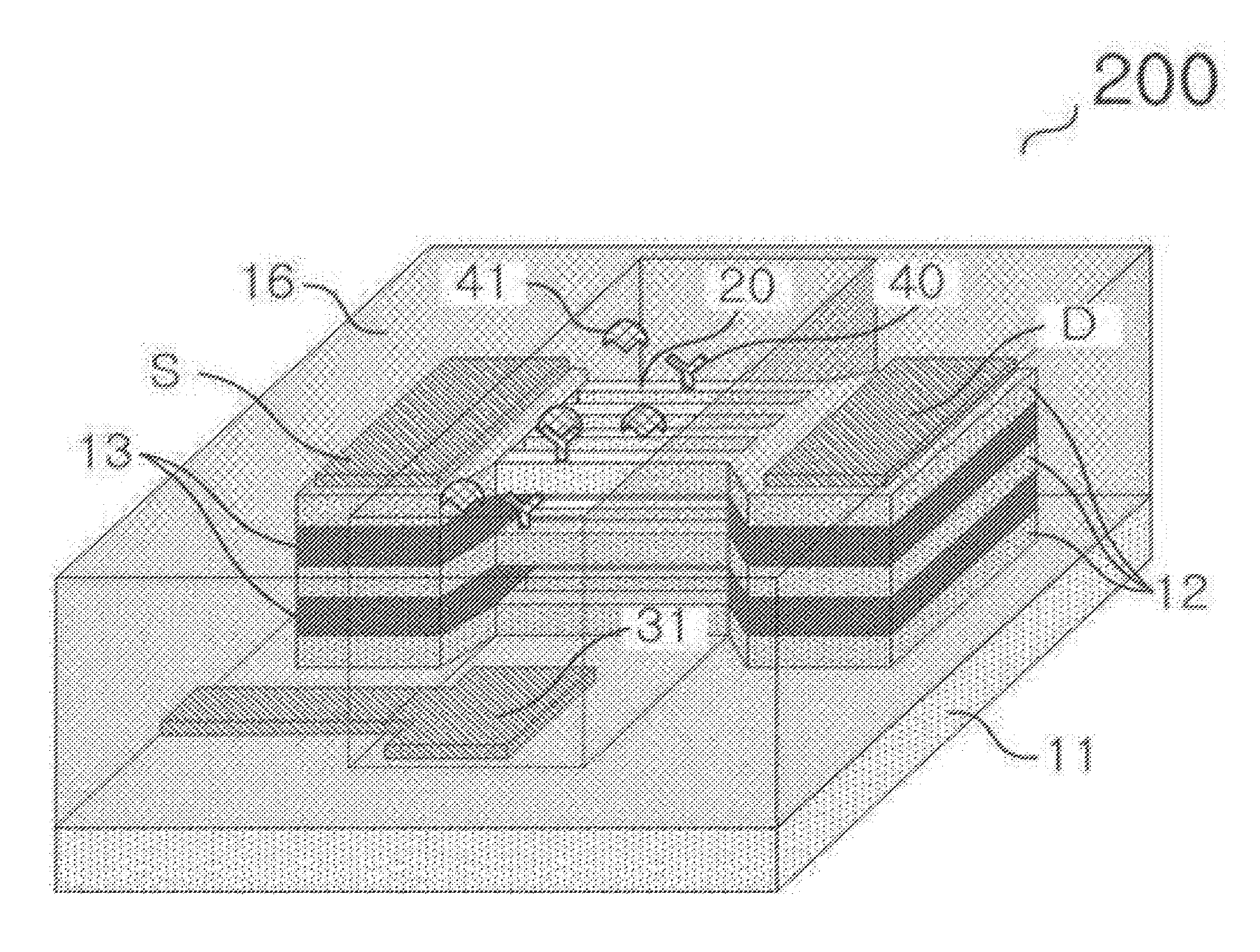
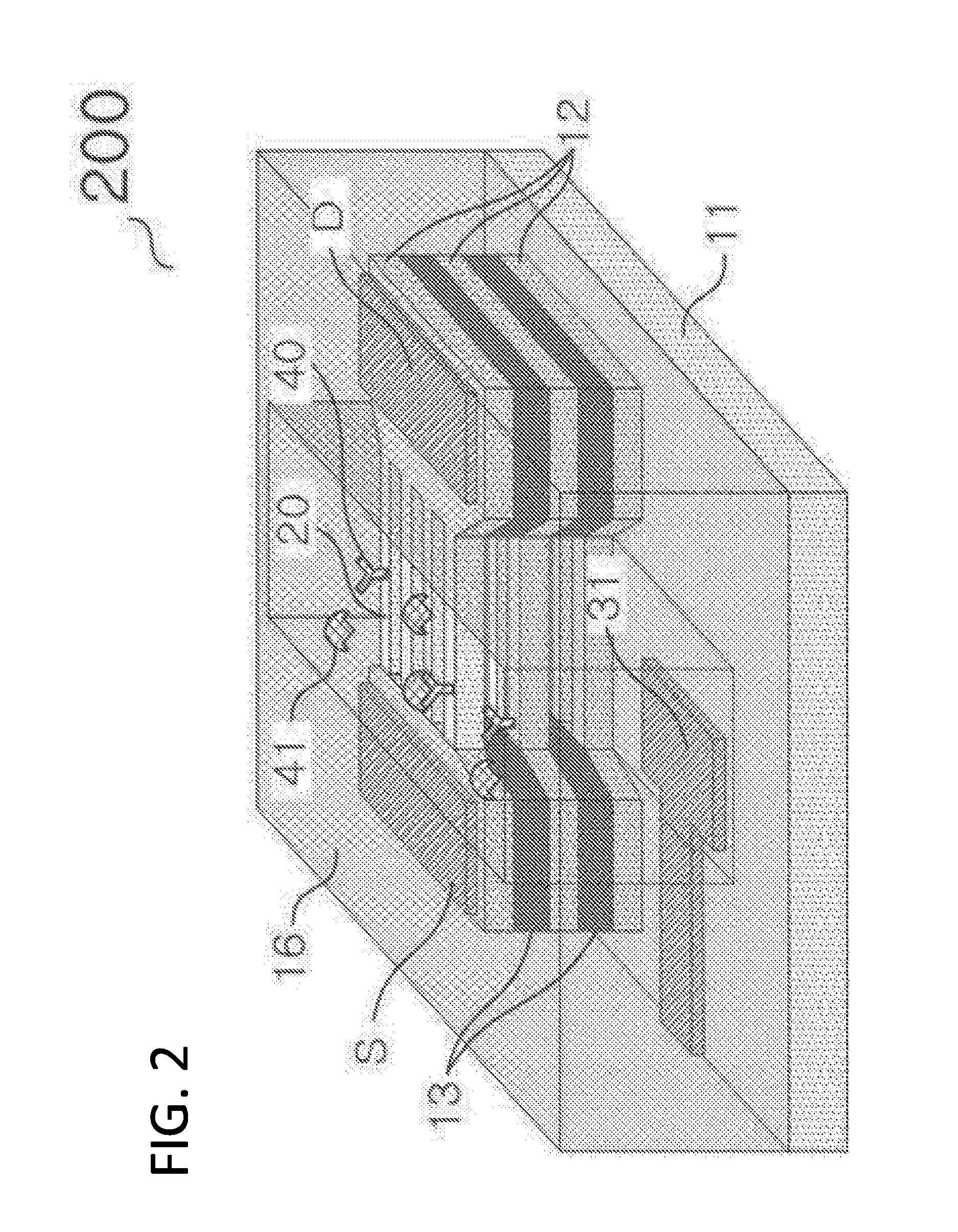
[0031]FIG. 2 illustrates the structure of a nanowire sensor having a three-dimensional stacked nanowire structure according to the present invention.

[0032]Referring to FIG. 2, the nanowire sensor having a three-dimensional stacked nanowire structure according to the present invention is fabricated using a semiconductor stack of a semiconductor channel layer 12 and a sacrificial layer 13 made of either a dielectric material or a semiconductor that can be etched selectively with respect to the channel layer. In the semiconductor stack, the channel layer 12 and sacrificial layer 13 in a patterned nanowire portion are etched, and then the sacrificial layer 13 in the nanowire portion is selectively etched so that the interlayer contact between the nanowires will not occur. Herein, the layers of each of the source S and the drain D should be electricall...


PUM

PropertyMeasurementUnit
widthaaaaaaaaaa
threshold voltageaaaaaaaaaa

Abstract

The present invention provides a nanowire sensor comprising nanowires, in which the nanowires are stacked to form a three-dimensional structure so that they have a large exposed surface area compared to that of a conventional straight nanowire sensor in the same limited area, thereby increasing the probability of attachment of a target material to the nanowires to thereby increase the measurement sensitivity of the sensor. Thus, a change in the electrical conductivity (conductance or resistance) of the nanowires can be sensed with higher sensitivity, suggesting that the sensor has increased sensitivity.

Description

TECHNICAL FIELD[0001]The present invention relates to a field effect sensor comprising nanowires, and more particularly, to a nanowire field effect sensor comprising nanowires having a three-dimensional stacked structure, in which the nanowires are stacked on a substrate in a direction perpendicular to the substrate so that a larger sensing area can be obtained in a limited substrate area.BACKGROUND ART[0002]Electrochemical sensors are devices that change the electrochemical properties of the material to be changed to electrical signals. Electrochemical sensors are expected to be widely used as biosensors and chemical sensors depending on the kind of target material to be sensed.[0003]For the detection and analysis of a material by an electrochemical sensor, the electrochemical sensor should is required to have high sensitivity so that a great change in the signal thereof can appear even when the target material have fine electrochemical properties. Further, the area of the electroc...

Claims


Application Information

Patent Timeline
Patent Type & Authority Applications(United States)
IPC IPC(8): H01L29/775G01N27/414H01L29/66
CPCH01L29/775G01N27/4146H01L29/66439G01N27/4145G01N27/414
Inventor LEE, JEONG SOOJEONG, YOON HAKIM, SUNG HOKIM, KI HYUNRIM, TAI UKBAEK, CHANG KI
Owner POSTECH ACAD IND FOUND
Why Eureka
Try Eureka