

Solid-state image sensing device and solid-state image pickup unit including same
- Summary
- Abstract
- Description
- Claims
- Application Information
AI Technical Summary
Benefits of technology
Problems solved by technology
Method used
Image

Examples
embodiment
Configuration of Image Pickup Device 10
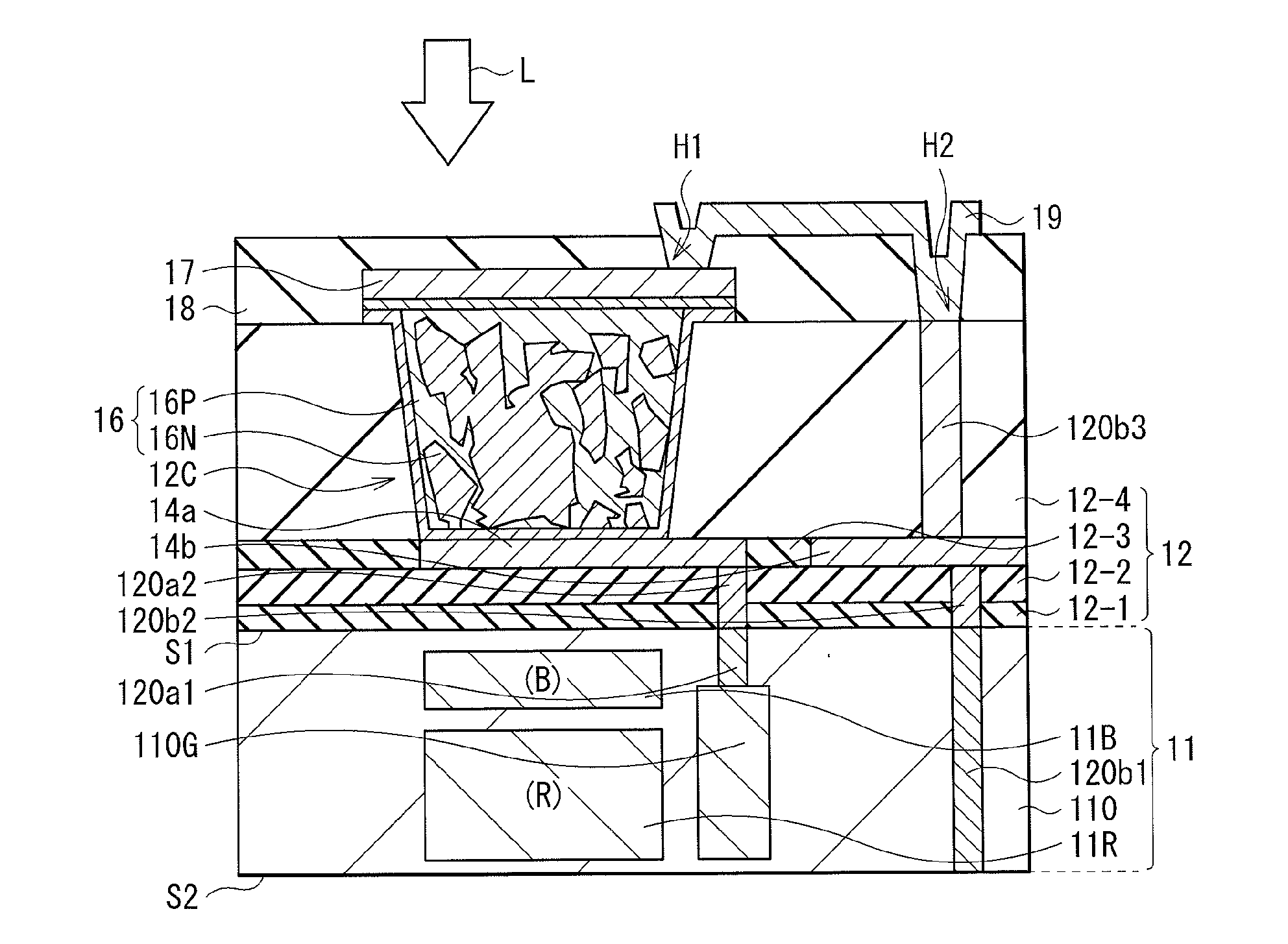
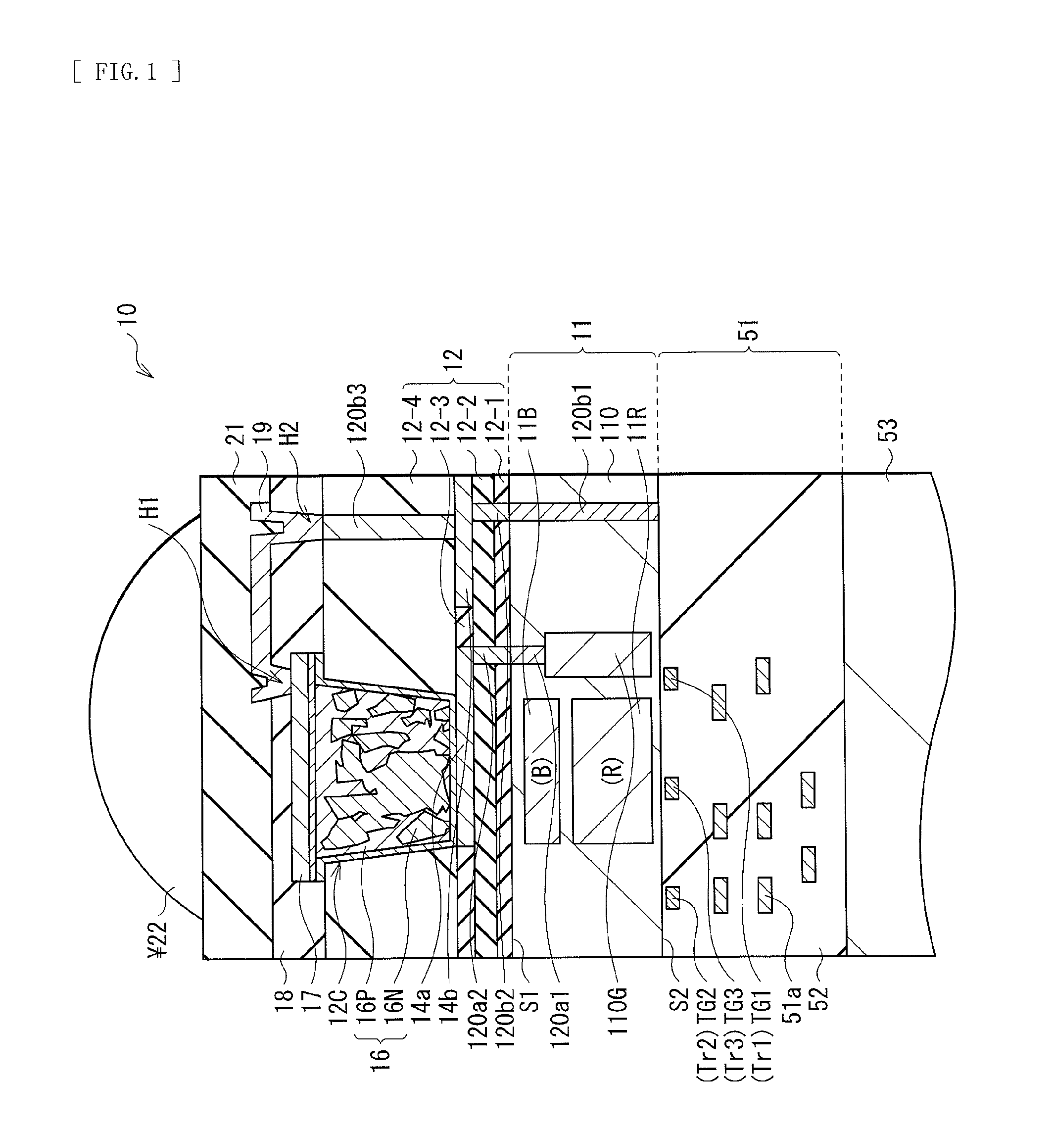
[0042]FIG. 1 illustrates a cross-sectional configuration of an image pickup device (an image pickup device 10) according to an embodiment of the present technology. The image pickup device 10 may form, for example, one pixel (for example, a pixel P in FIG. 20 described later) in an image pickup unit (e.g. an image pickup unit 1 in FIG. 20 described later) such as a CCD image sensor and a CMOS image sensor. The image pickup device 10 is of a backside-illumination type, in which a multilayered wiring layer 51 is provided on a surface (a surface S2) opposite to a light-receiving surface (a surface S1) of a semiconductor substrate 11.
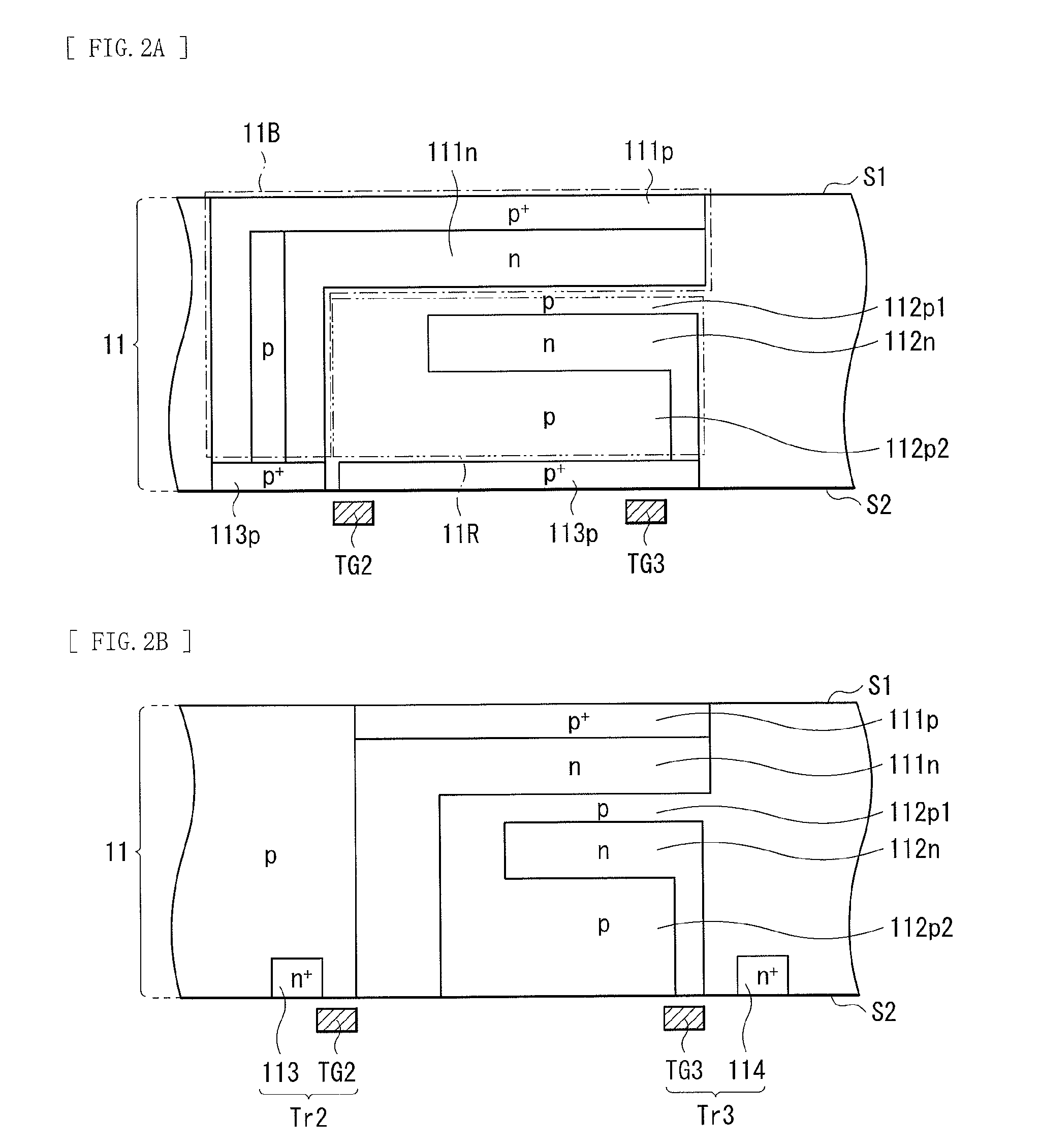
[0043]The image pickup device 10 includes inorganic photoelectric conversion sections 11B and 11R (a second photoelectric conversion section) and an organic photoelectric conversion section 16 (a first photoelectric conversion section), which are laminated in a vertical direction (an optical path). The inorganic photoe...
modification 1
[0091]FIG. 16 illustrates a cross-sectional configuration of an image pickup device (an image pickup device 10A) according to a modification 1 of the above-described embodiment. In the image pickup device 10A, the interlayer insulating film (the interlayer insulating layer 12-2) is not present between the lower electrode 14a and the interlayer insulating layer 12-1. The image pickup device 10A is otherwise similar to the image pickup device 10 in terms of configuration, functions, and effects.
[0092]In the image pickup device 10A, the lower electrode 14a is in contact with the interlayer insulating layer 12-1, and the insulating film between the semiconductor substrate 11 and the organic photoelectric conversion section 16 is minimized. This makes it possible to reduce reflection when light travels from the organic photoelectric conversion section 16 to the inorganic photoelectric conversion section 11B, thereby further increasing the photoelectric conversion efficiency.
modification 2
[0093]FIG. 17 illustrates a cross-sectional configuration of an image pickup device (an image pickup device 10B) according to a modification 2 of the above-described embodiment. In the image pickup device 10B, a lower electrode (a lower electrode 24a) is provided in in the depression section 12C, together with the photoelectric conversion section 16. The image pickup device 10B is otherwise similar to the image pickup device 10 in terms of configuration, functions, and effects.
[0094]In the image pickup device 10B, it is possible to omit the interlayer insulating layer 12-3, and the interlayer insulating layer 12-4 having the depression section 12C is provided on the interlayer insulating layer 12-2. The lower electrode 24a is provided along the sidewall and the bottom of the depression section 12C in the interlayer insulating layer 12-4. The green storage layer 110G may be disposed at any position, and may be provided opposite the conductive plug 120b1 (FIG. 17), or may be provided ...
PUM
 Abstract
Description
Claims
Application Information