Printed antenna having non-uniform layers

Inactive Publication Date: 2015-10-29
VAYYAR IMAGING LTD
View PDF3 Cites 26 Cited by
  • Summary
  • Abstract
  • Description
  • Claims
  • Application Information

AI Technical Summary

Benefits of technology

[0010]It is an objective of the present invention to provide printed circuit antennas with low

Problems solved by technology

Since space is limited in the ever-decreasing size of today's devices, such antenna traces are typically formed near one or more ground planes formed on the same PCB.
In such arrangements, a portion of the PCB substrate, typically the area of a PCB having the highest density of electromagnetic energy, remains in between the antenna and the ground plane, impacting antenna efficiency and bandwidth.
More specifically, as radio

Method used


Image

  • Printed antenna having non-uniform layers
  • Printed antenna having non-uniform layers
  • Printed antenna having non-uniform layers

Examples


Embodiment Construction

[0037]The present invention relates to printed antennas for radiating and receiving electromagnetic waves and, more particularly to a low profile, printed antenna comprising non-uniform dielectric layers.

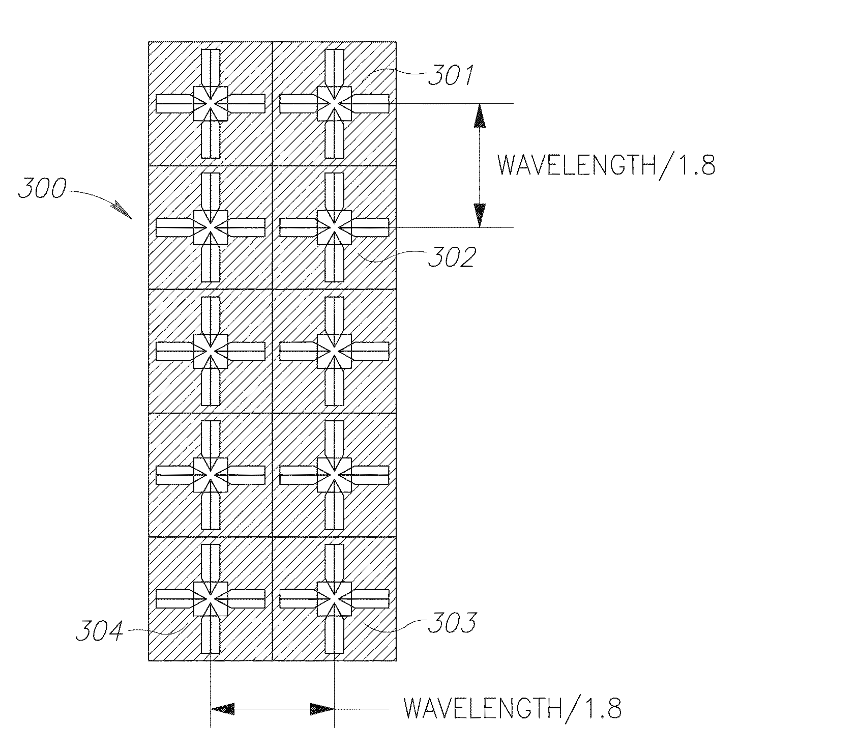
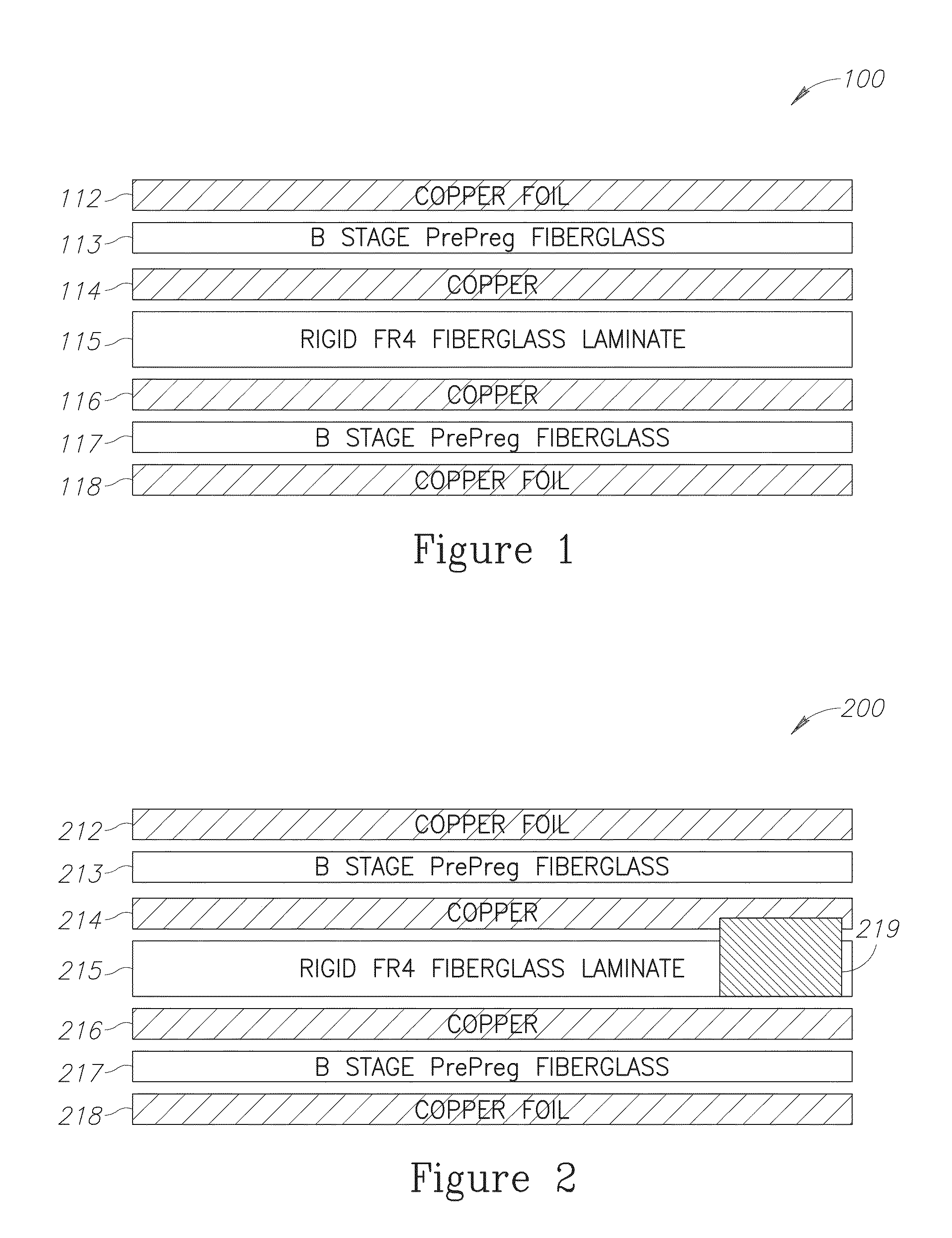
[0038]As illustrated in FIG. 1, an antenna such as PCB based antennas design and manufacturing methods used by prior art include a plurality of uniform dielectric layers included in the PCB multi-layer antenna. For example a low loss dielectric materials such as glass-epoxy or Teflon is used to entirely and or laterally fill the space between each pair of conducting layers.

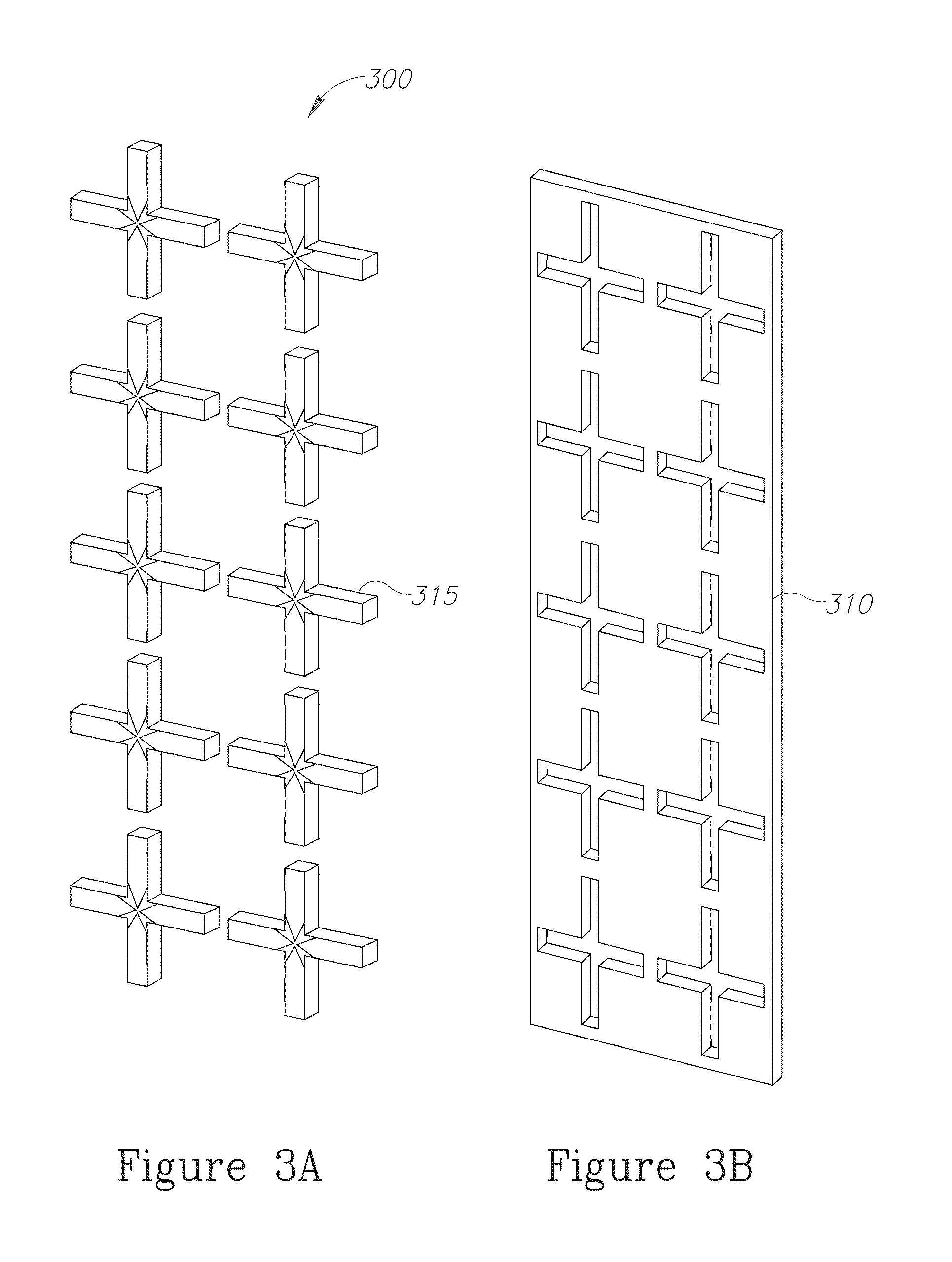
[0039]The present invention provides a printed antenna, such as a multi-layer antenna comprising one or more non-uniform dielectric layers. More specifically the present invention provides a printed antenna comprising a plurality of dielectric layers, and a plurality of conducting layers, wherein at least one of the antenna's dielectric layer contains regions, such as lateral regions or sections with differing die...


PUM


Abstract

An antenna has a plurality of dielectric layers and a plurality of conducting layers. At least one of the dielectric layers comprises one or more regions with differing dielectric properties. A plurality of such antennas may be arranged in an antenna array. The array includes a radiating component etched in the array top first layer, a reflector embedded in a second layer below the top layer, a feeding network located in a third layer below the reflector, and a ground plane bottom layer configured to shield the feeding network in the bottom layer. At least one of the layers of the array is a non-uniform dielectric layer of a material having a substantially different electrical property compared to the array dielectric and conducting layers.

Description

FIELD OF THE INVENTION[0001]The present invention relates to printed antennas for radiating and receiving electromagnetic waves and, more particularly to a low profile, printed circuit board (PCB) antenna.BACKGROUND INFORMATION[0002]Printed antennas such as PCB based antennas as known in the art may include a plurality of layers having various shapes, size and thickness, where each layer is interconnected with conductive vias, to further provide electrical connections for complex electronic circuitry. Conventional PCBs include a rigid substrate to provide support for mounting electronic components in communications and sensing devices. In addition, conductive materials are plated over such substrates and etched to provide electrically conductive traces for interconnecting these components.[0003]For many devices, antennas are typically formed on the same PCBs, which also carry transmitting and receiving radio frequency (RF) circuitry. A common technique employed to form antennas on P...

Claims


Application Information

Patent Timeline
IPC IPC(8): H01Q9/04H01Q21/06H01Q19/10
CPCH01Q9/0407H01Q21/06H01Q19/10H01Q1/48H01Q1/523H01Q19/108H01Q21/062H01Q21/26
Inventor GOLOMBEK, HAREL
Owner VAYYAR IMAGING LTD
Why Eureka
Try Eureka