High-frequency switch module

a high-frequency switch and module technology, applied in transmission, multiple-port network, electrical equipment, etc., can solve the problems of difficult to reduce the size of the high-frequency circuit, radio wave interference, degradation of the out-of-band characteristics of the high-frequency switch module, etc., to achieve excellent harmonic distortion characteristics and out-of-band characteristics, the effect of reducing the siz

Active Publication Date: 2015-11-05
MURATA MFG CO LTD
View PDF4 Cites 25 Cited by
  • Summary
  • Abstract
  • Description
  • Claims
  • Application Information

AI Technical Summary

Benefits of technology

[0037]With this configuration, a high-frequency switch module which allows an appropriate amount of phase adjustment to be easily realized and enables reduction in size is provided.
[0038]According to various preferred embodiments of the present invention, a small-sized high-frequency switch module having excellent harmonic distortion characteristics and out-of-band characteristics is easily realized.

Problems solved by technology

Such harmonic signals being transmitted to the outside from the common terminal through an antenna causes various problems such as radio wave interference and the like to be generated.
In other words, such harmonic signals due to distortion cause degradation of the out-of-band characteristics of the high-frequency switch module.
This makes it difficult to reduce the size of the high-frequency circuit.
Further, it is not easy to determine the length and conductor pattern of the signal transmission line for obtaining the optimum amount of phase shift under the constraint of the shape as the multilayer module of the high-frequency circuit.
Hence, with the existing configuration disclosed in Japanese Unexamined Patent Application Publication No. 2001-86026, it is difficult to facilitate realization of, and reduction in the size of, a high-frequency circuit which includes a switch IC and has excellent harmonic distortion characteristics and out-of-band characteristics.

Method used


Image

  • High-frequency switch module
  • High-frequency switch module
  • High-frequency switch module

Examples


Embodiment Construction

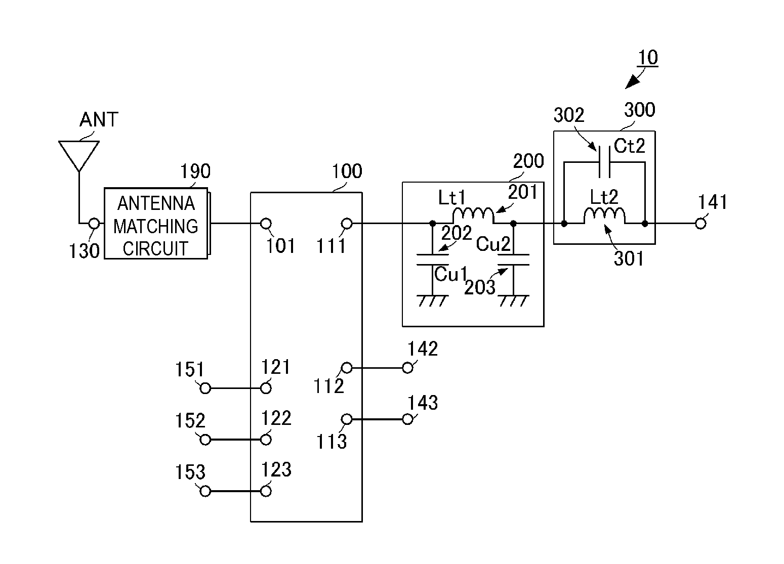
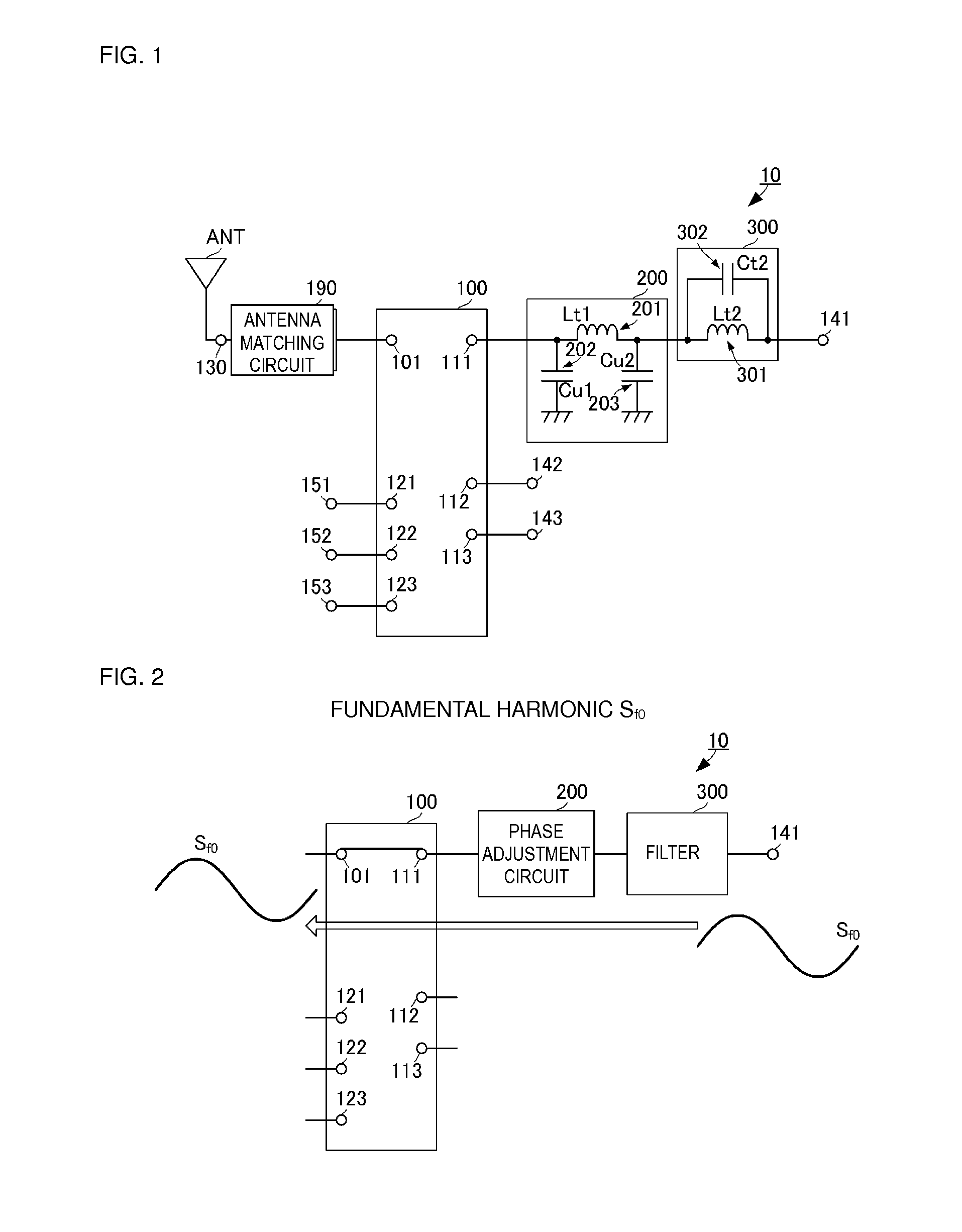
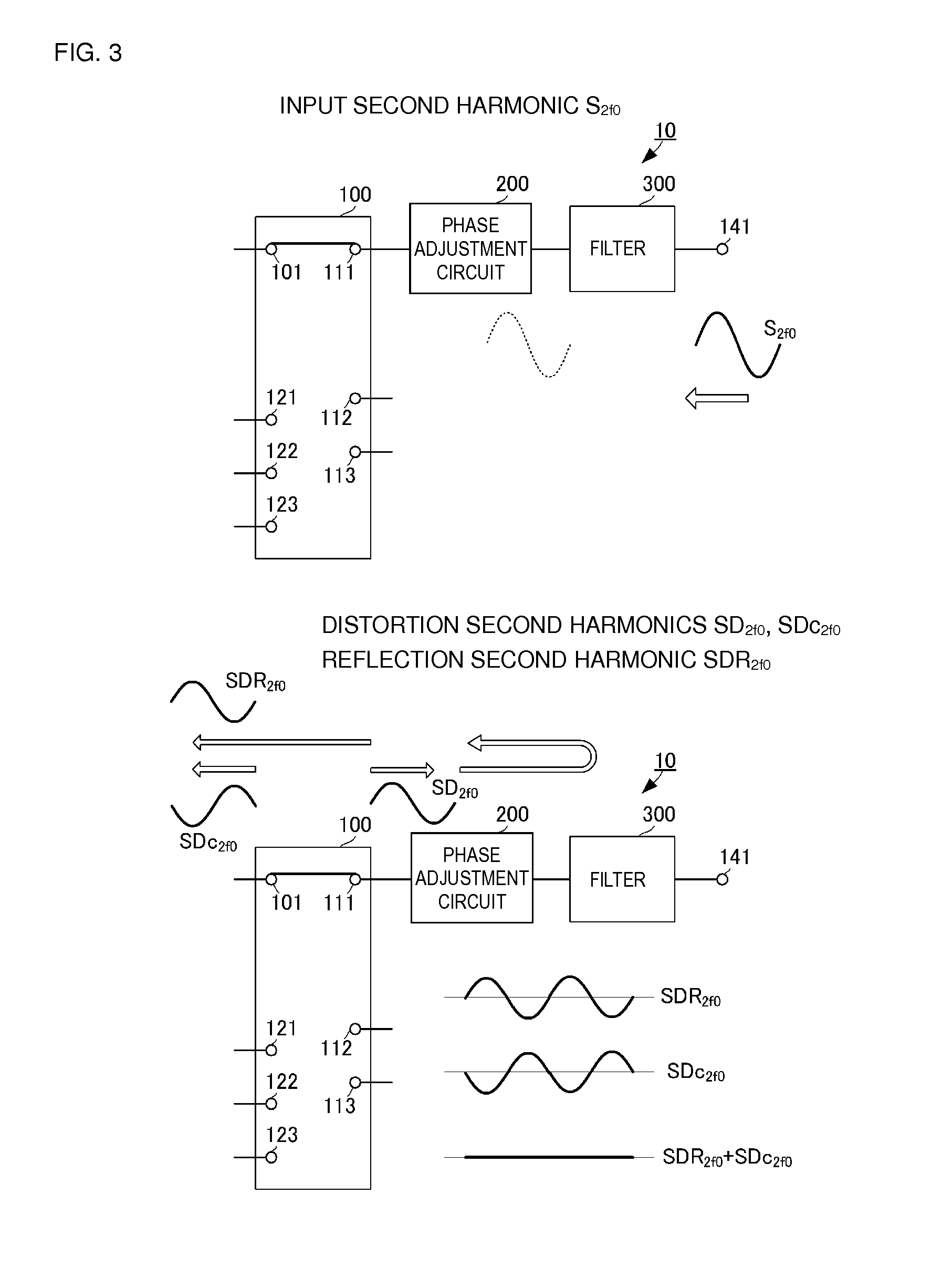
[0055]A high-frequency switch module according to a first preferred embodiment of the present invention will be described with reference to the drawings. FIG. 1 is a circuit diagram of the high-frequency switch module according to the first preferred embodiment of the present invention. Note that in the present preferred embodiment a switch IC having a single common terminal and three individual terminals will be described as an example. However, the number of the individual terminals is not limited to this, and may be any number other than one.

[0056]A high-frequency switch module 10 includes a switch IC 100, a phase adjustment circuit 200, a filter 300, and an antenna matching circuit 190. The high-frequency switch module 10 includes external connection terminals 130, 141, 142, 143, 151, 152, and 153. The external connection terminal 141 corresponds to the “first external connection terminal”. The external connection terminal 130 is connected to an antenna ANT arranged outside of t...


PUM


Abstract

A high-frequency switch module includes a switch IC, a phase adjustment circuit, and a filter circuit. The phase adjustment circuit, which includes an inductor and capacitors, includes a π-type circuit in which the inductor is connected in series between an individual terminal and the filter circuit. The filter circuit is an LC parallel resonant circuit including a filter inductor and a filter capacitor. A distortion second harmonic signal from the individual terminal of the switch IC is reflected by the filter circuit through the phase adjustment circuit and returns to the switch IC through the phase adjustment circuit. This distortion second harmonic signal, whose phase is adjusted by the phase adjustment circuit, is cancelled out by a distortion second harmonic signal output to a common terminal of the switch IC.

Description

BACKGROUND OF THE INVENTION[0001]1. Field of the Invention[0002]The present invention relates to a high-frequency switch module that transmits and receives a plurality of types of high-frequency signals by connecting a common terminal to one of a plurality of individual terminals by using a semiconductor switch.[0003]2. Description of the Related Art[0004]Various types of high-frequency switch modules for transmitting and receiving a plurality of high-frequency signals by using a common antenna have been devised. In such a high-frequency switch module, there is a case in which a switch IC including a common terminal and a plurality of individual terminals is used. The switch IC includes a plurality of field-effect transistors (FETs) and connects the common terminal to one of the individual terminals through the on / off operations of the FETs.[0005]In such a switch IC that uses a semiconductor, harmonic signals due to distortion are generated when a high-power high-frequency signal (t...

Claims


Application Information

Patent Timeline
Patent Type & Authority Applications(United States)
IPC IPC(8): H04B1/48
CPCH04B2001/485H04B1/48H03H7/0115H03H7/19H03H7/21H03H7/463H03H2001/0085H03H2007/013H04B1/0057H04B1/0458H04B1/18
Inventor UEJIMA, TAKANORI
Owner MURATA MFG CO LTD
Why Eureka
Try Eureka