Storage device, memory cell, and data writing method

a storage device and memory cell technology, applied in the field of storage devices, memory cells, and data writing methods, can solve the problems of increasing power consumption in these areas, and achieve the effect of high-speed writing

Active Publication Date: 2015-11-19
TOHOKU UNIV
View PDF1 Cites 8 Cited by
  • Summary
  • Abstract
  • Description
  • Claims
  • Application Information

AI Technical Summary

Benefits of technology

[0050]In accordance with the present disclosure, there can be provided a storage device which is small and is capable of high-speed writing, and in which little current is passed during stand-by; a memory cell; and a data writing method.

Problems solved by technology

There is a problem that as integrated circuits becomes finer (scaling) and the integrated circuits have a higher capacity, the off-state leakage current of a transistor such as a MOSFET which is a basic element of the integrated circuits, e.g. SRAM (FIG. 27), increases, resulting in increased power consumption therein.

Method used


Image

  • Storage device, memory cell, and data writing method
  • Storage device, memory cell, and data writing method
  • Storage device, memory cell, and data writing method

Examples


first embodiment

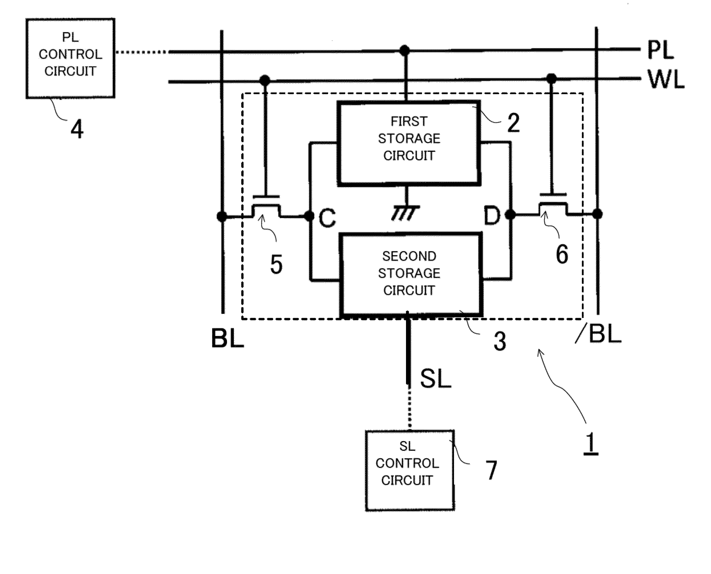
[0090]FIG. 1 illustrates the circuit configuration comprising a memory cell 1 according to a first embodiment of the present disclosure. The memory cell 1 comprises a first storage circuit 2, a second storage circuit 3, a first transfer MOSFET 5 (metal oxide semiconductor field effect transistor), and a second transfer MOSFET 6.

[0091]A time (hereinafter, write time) necessary for writing data on the first storage circuit 2 is t1, and the write time of the second storage circuit 3 is t2. In this case, t12 is satisfied. In other words, data can be written on the first storage circuit 2 at a higher speed than on the second storage circuit 3. A time (hereinafter, data retention time) for which the first storage circuit 2 can retain data is τ1, the data retention time of the second storage circuit 3 is τ2, and τ12 is satisfied. In other words, the second storage circuit 3 can retain data over a longer period than the first storage circuit 2. For example, the first storage circuit 2 may b...

second embodiment

[0118]An example of a storage device in which the memory cell 1 mentioned above is used will be explained below.

[0119]In the storage device 20 according to a second embodiment, the memory cell 1 according to the first embodiment is used. The storage device 20 carries out power gating for supplying power to memory cells 1 on the basis of a group (hereinafter, grain) including the plural memory cells 1 as a unit.

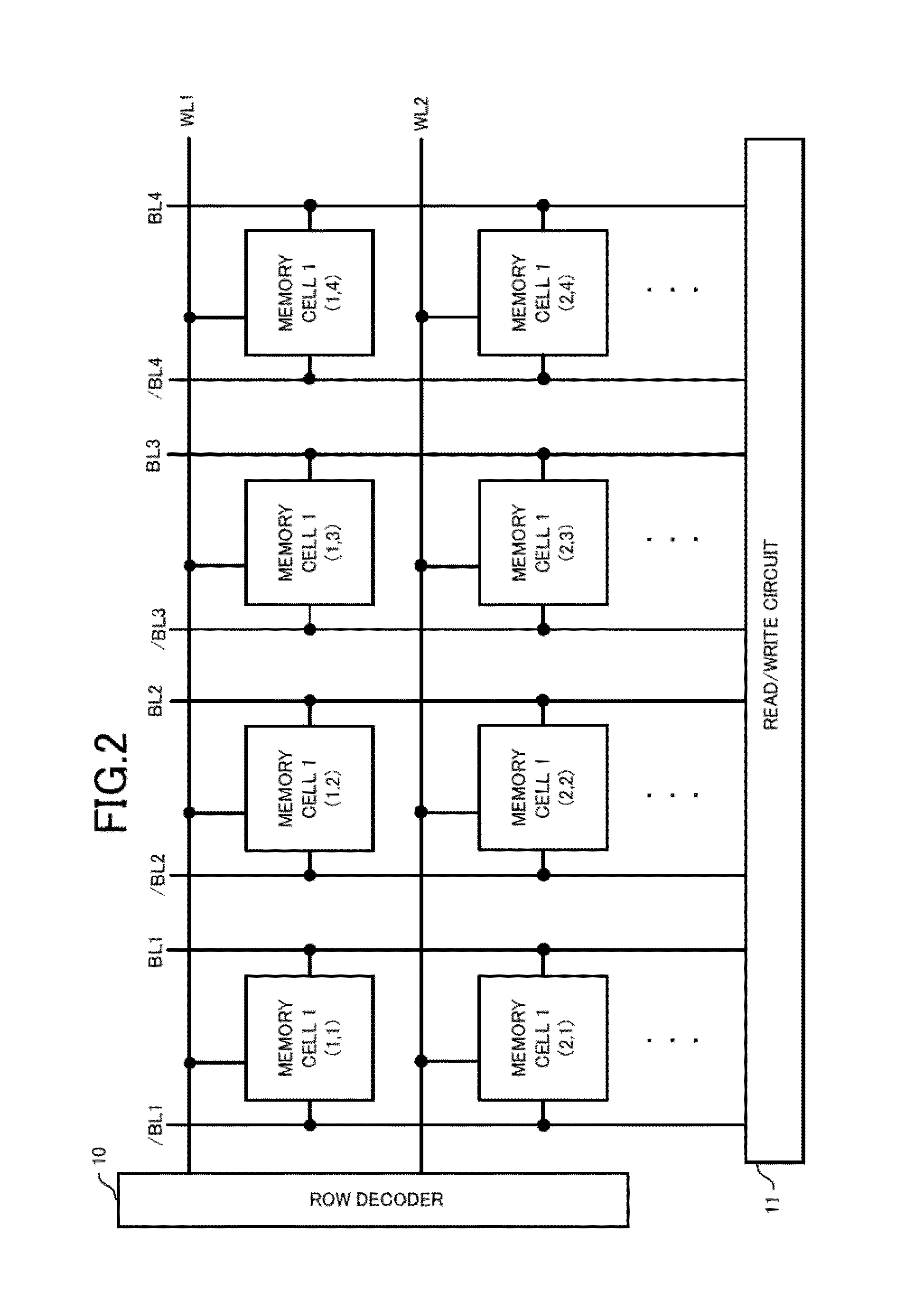
[0120]FIG. 4 is a block diagram illustrating the configuration of a grain 25 included in the storage device 20. The grain 25 includes 2N memory cells 1 on the same word line (N is an integer). For example, 2N is 16, 32, 64, or the like. The configuration of the memory cell 1 is similar to that of the first embodiment. The reading and writing methods of the memory cell 1 are also similar to those of the first embodiment.

[0121]A PL control circuit 4 is assigned to each grain 25. The PL control circuit 4 and each memory cell 1 are connected to each other via a power line PL. The ...

specific example of first embodiment

[0144]A specific example of the memory cell 1 used in the storage device 20 illustrated in FIG. 4 will be explained below.

[0145]FIG. 11 is a circuit diagram of the specific example of the memory cell 1. FIG. 12 is a timing chart.

[0146]In such a case, the first storage circuit 2 comprises a so-called SRAM, and the second storage circuit comprises MTJ elements 30 and 31.

[0147]The first storage circuit 2 comprises a first inverter 12, a first transfer n-type MOSFET 5 connected to the first inverter 12, a second inverter 14, and a second transfer n-type MOSFET 6 connected to the second inverter 14.

[0148]The first inverter 12 comprises a first p-type MOSFET 16 as a load and a first driving n-type MOSFET 17. The drain of the first driving n-type MOSFET 17 is connected to the drain of the first p-type MOSFET 16, and the source of the first driving n-type MOSFET 17 is grounded. The gate of the first driving n-type MOSFET 17 is connected to one end of the main electrode of the second transfe...


PUM


Abstract

A memory cell (1) includes a first storage circuit (2) with a write time t1 and a data retention time τ1 and a second storage circuit (3) with a write time t2 and a data retention time τ2 (t1<t2 and τ12). A row decoder supplies write data to the memory cell (1) via a word line (WL) to write the data on the first storage circuit (2) over a write time tW that is longer than the write time t1 and that is shorter than the write time t2. A PL control circuit (4) supplies power to the memory cell (1) for a time that is longer than the write time t2 when the write data is supplied to the memory cell (1), writes, on the second storage circuit (3), the data written on the first storage circuit (2) once the supply of the write data is stopped, and stops the supply of the power to the memory cell (1) after a lapse of the write time t2 following start of the supply of the write data.

Description

TECHNICAL FIELD[0001]The present disclosure relates to storage devices, memory cells, and data writing methods. More specifically, the present disclosure relates to a storage device in which a resistance-change-type storage element is used, a memory cell, and a data writing method.BACKGROUND ART[0002]There is a problem that as integrated circuits becomes finer (scaling) and the integrated circuits have a higher capacity, the off-state leakage current of a transistor such as a MOSFET which is a basic element of the integrated circuits, e.g. SRAM (FIG. 27), increases, resulting in increased power consumption therein.[0003]Therefore, an attempt to power off an integrated circuit has been made to reduce an off-leak when information processing is not carried out in the integrated circuit. For example, there is a method in which data stored in a volatile storage circuit and / or the like included in an integrated circuit is saved into a storage element with a long data retention time prior ...

Claims


Application Information

Patent Timeline
Patent Type & Authority Applications(United States)
IPC IPC(8): G11C7/22G11C11/16G11C13/00
CPCG11C7/22G11C11/1675G11C13/0069G11C13/0004G11C14/0081G11C14/009G11C13/0007G11C11/1655G11C11/1659G11C11/1673G11C11/1693G11C11/1657
Inventor OHSAWA, TAKASHIENDOH, TETSUO
Owner TOHOKU UNIV
Why Eureka
Try Eureka