Method and System of Creating a Symmetrical FIB Deposition

Inactive Publication Date: 2015-12-24
FEI COMPANY
View PDF14 Cites 15 Cited by
  • Summary
  • Abstract
  • Description
  • Claims
  • Application Information

AI Technical Summary

Benefits of technology

The invention provides a method and apparatus for producing symmetrical beam-induced deposition when using a charged particle beam that is incident at a non-normal angle to the work piece surface. This can be used to form a protective layer as part of a process of forming a lamella for viewing on a transmission electron microscope. The system and methods can be used to set the operational parameters, including beam energy and scan direction, to provide the symmetrical deposition. The invention allows for the use of a non-orthogonal angle between the charged particle beam and the work piece surface, resulting in a more symmetrical deposition.

Problems solved by technology

Monitoring nanometer scale processes, such as the photolithography processes used in the fabrication of integrated circuits, is challenging.
As features continue to get smaller and smaller, however, there comes a point where the features to be measured are too small for the resolution provided by an ordinary SEM.
Because a sample must be very thin for viewing with transmission electron microscopy (whether TEM or STEM), preparation of the sample can be delicate, time-consuming work.
Because FIB milling can cause significant damage to small structures, the work piece surface is often coated with a protective layer of tungsten or carbon before milling begins.
SEM deposition of the protective layer can be used to protect sensitive surfaces from FIB damage, but this can lead to lamella placement issues unless a recognizable mark is visible to the FIB after the feature if interest has been covered with SEM deposition.

Method used


Image

  • Method and System of Creating a Symmetrical FIB Deposition
  • Method and System of Creating a Symmetrical FIB Deposition
  • Method and System of Creating a Symmetrical FIB Deposition

Examples


Embodiment Construction

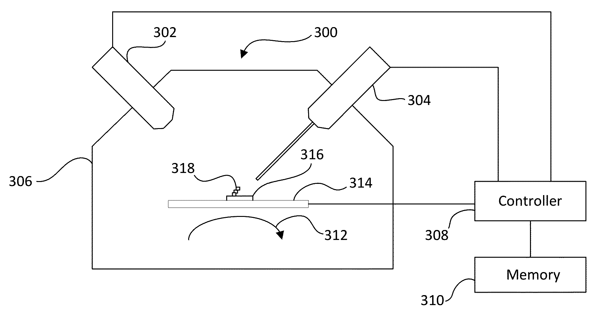
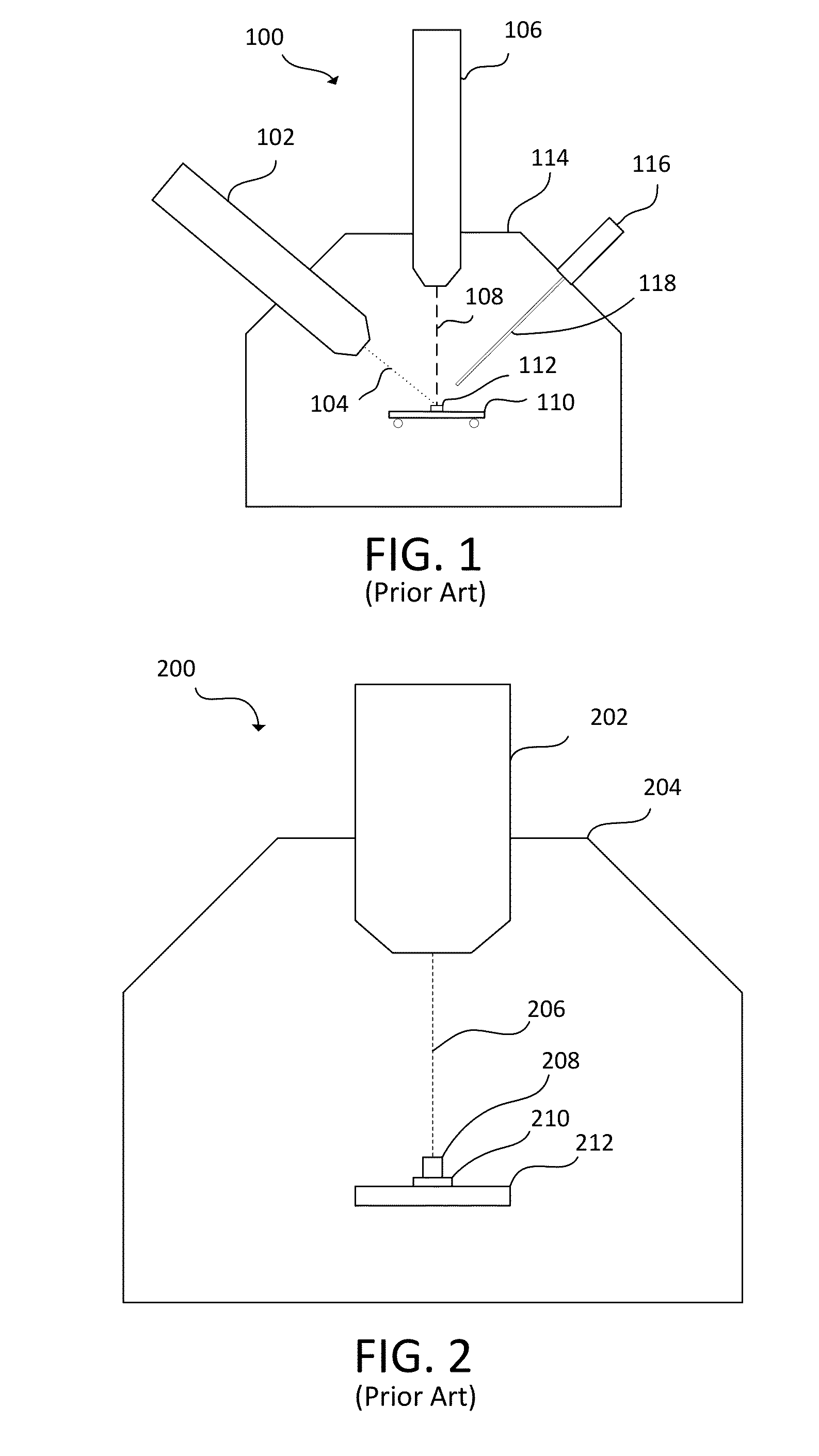
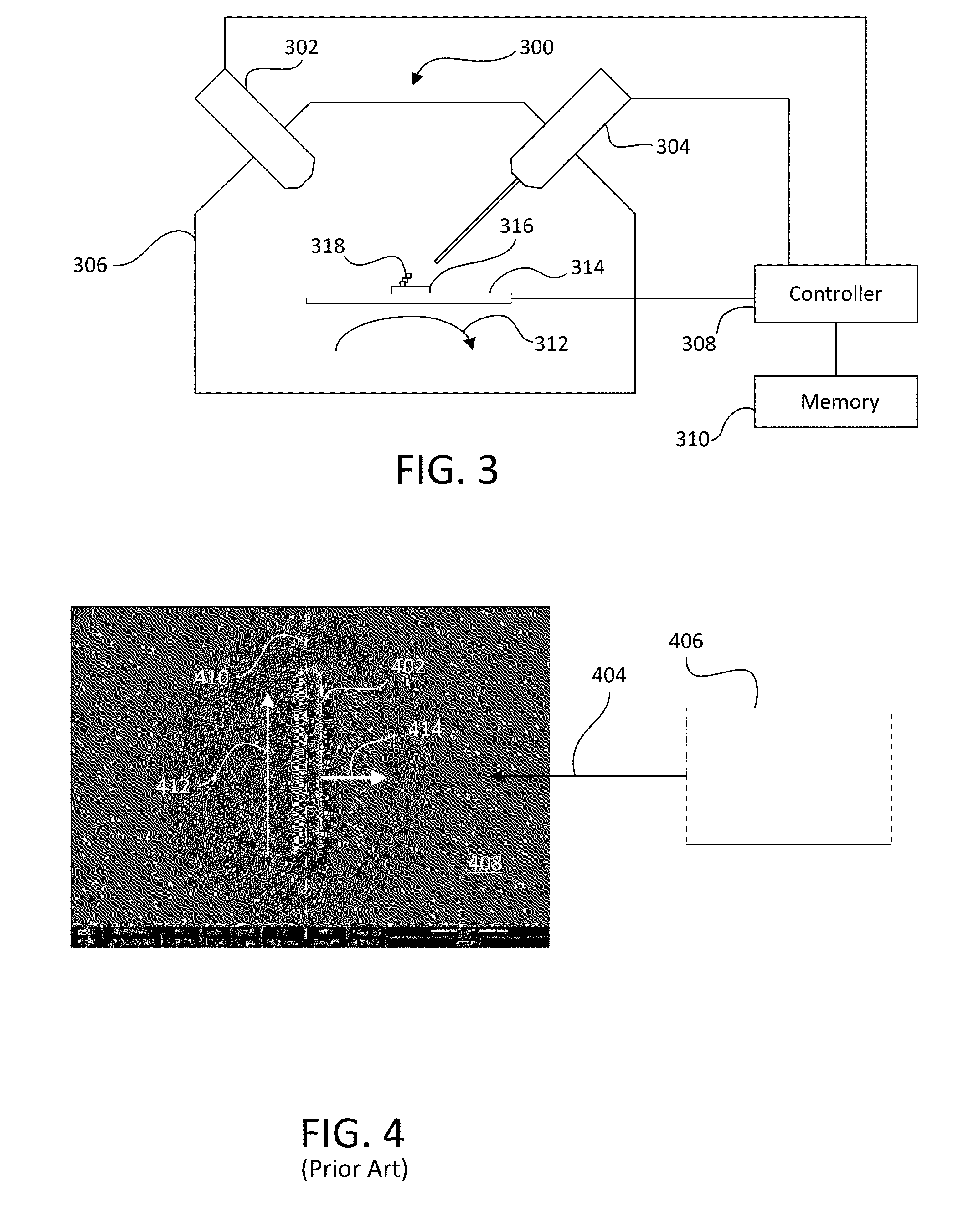
[0032]Preferred embodiments of the present invention are directed toward methods and apparatuses for improved beam-induced deposition with a beam that is not orthogonal to the work piece surface. Embodiments are particularly useful to provide improved control of the deposition of protective layers for lamella manufacture.

[0033]When a beam inducing a deposition is incident at a non-orthogonal angle to the work piece surface, the deposition tends to grow in the direction of the beam source instead of normal to the work piece surface, resulting in an asymmetrical deposit. This asymmetrical deposition adversely affects the quality of the subsequent milling steps through the deposited layer because regions with a thicker protective layer will etch more slowly. The asymmetrical deposition is thought to be caused by the mechanics of the beam-induced deposition process. During a focused ion beam deposition process, there is competition between deposition and sputtering, and the sputtering r...


PUM

PropertyMeasurementUnit
Fractionaaaaaaaaaa
Angleaaaaaaaaaa
Angleaaaaaaaaaa

Abstract

A system is provided to produce symmetric depositions using a charged-particle beam deposition with an angled beam. In the past, the use of an FIB with non-orthogonal incidence angles produced depositions that grew toward the FIB beam path making it difficult to produce uniformity of the deposit. With the current invention, a symmetrical deposition is made even with the use of a non-orthogonal FIB.

Description

[0001]This application claims priority from U.S. Prov. Pat. App. No. 62 / 016,464, filed Jun. 24, 2014, which is hereby incorporated by reference.TECHNICAL FIELD OF THE INVENTION[0002]The present invention relates to charged particle beam-induced deposition and more specifically to deposition processes in which beam is not orthogonal to the work piece surface.BACKGROUND OF THE INVENTION[0003]Monitoring nanometer scale processes, such as the photolithography processes used in the fabrication of integrated circuits, is challenging. To fabricate integrated circuits, a semiconductor substrate, such as silicon wafer, on which circuits are being formed is coated with a material, such as a photoresist, that changes solubility when exposed to radiation. A lithography tool, such as a mask or reticle, positioned between the radiation source and the semiconductor substrate casts a shadow to control which areas of the substrate are exposed to the radiation. After the exposure, the photoresist is ...

Claims


Application Information

Patent Timeline
IPC IPC(8): G01N1/32H01J37/305G03F7/20C23C16/48C23C16/50C23C16/52H01J37/302H01J37/317
CPCG01N1/32H01J37/3023H01J37/3056H01J37/3178C23C16/486C23C16/50H01J2237/31732G03F7/70616H01J2237/006H01J2237/049H01J2237/304H01J2237/31745H01J2237/31749C23C16/52H01J2237/3109H01J37/317
Inventor FULLER, SCOTT EDWARDSIDOROV, OLEG
Owner FEI COMPANY
Why Eureka
Try Eureka