Predicting circuit reliability and yield using neural networks

a neural network and circuit reliability technology, applied in the direction of program control, total factory control, instruments, etc., can solve the problems of high cost of manufacturing semiconductor devices, inability to assess reliability risk and yield, and inability to take corrective action to correct defects. end-of-line testing may be too late to achieve the effect of ensuring reliability and yield

Inactive Publication Date: 2015-12-24
SEMICON MFG INT (SHANGHAI) CORP
View PDF8 Cites 22 Cited by
  • Summary
  • Abstract
  • Description
  • Claims
  • Application Information

AI Technical Summary

Benefits of technology

[0006]Embodiments of the present invention provide a predictive system and method for predicting reliability risk and yield performance of manufactured semiconductor devices that can prevent reliability and yield problems from occurring during a manufacturing process of semiconductor devices according to inline real-time data acquisition.

Problems solved by technology

Currently, the assessment of reliability risk and yield can only be obtained through testing of fully processed wafers or based on previously gained experience.
End-of-line testing may be too late to take corrective action to correct defects.
This results in potentially high risk because the fully processed wafers may have to be scrapped, causing increased costs of manufactured semiconductor devices.
The prior art does not provide an inline prediction capability to solve the problems related to reliability and yield of semiconductor devices.

Method used


Image

  • Predicting circuit reliability and yield using neural networks
  • Predicting circuit reliability and yield using neural networks
  • Predicting circuit reliability and yield using neural networks

Examples


embodiment 1

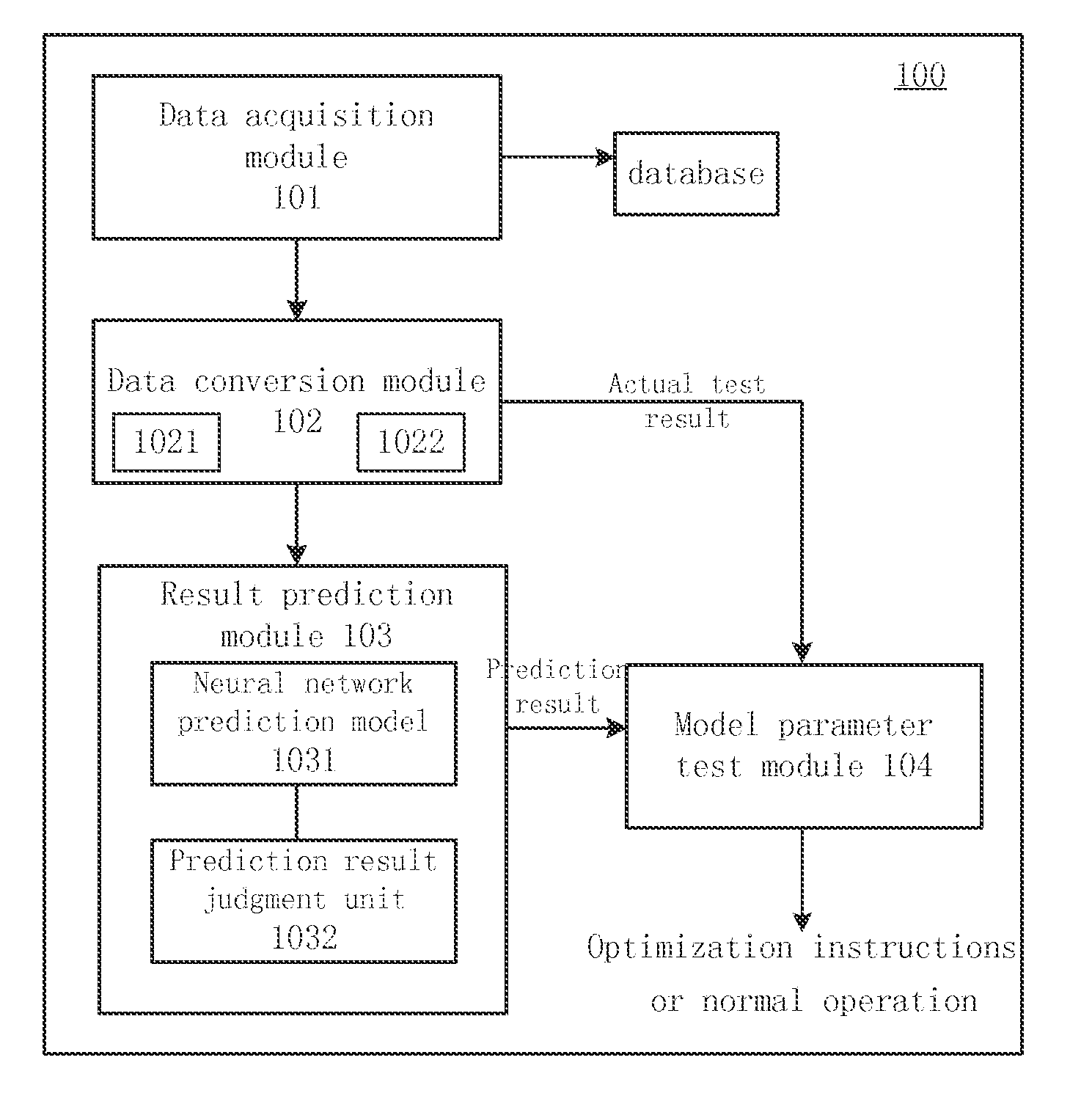
[0028]In accordance with the present invention, a system of predicting a semiconductor device manufacturing process can prevent problems related to reliability and yield of a semiconductor device based on a predicted result obtained through inline acquisition of data associated with to-be predicted prediction information. The prediction of reliability risk and yield may be implemented using a neural network module. The expression “inline acquisition of data” refers to acquisition of data within a manufacturing process.

[0029]Referring to FIG. 1, a system 100 (alternatively also referred to as “the system” or “the prediction system” throughout the description) for predicting reliability and / or yield of a semiconductor device may include a data acquisition module 101, a data conversion module 102, and a result prediction module 103. Result prediction module 103 may include a neural network prediction module 1031 and a prediction result judgment unit 1032. System 100 may also include a ...

embodiment 2

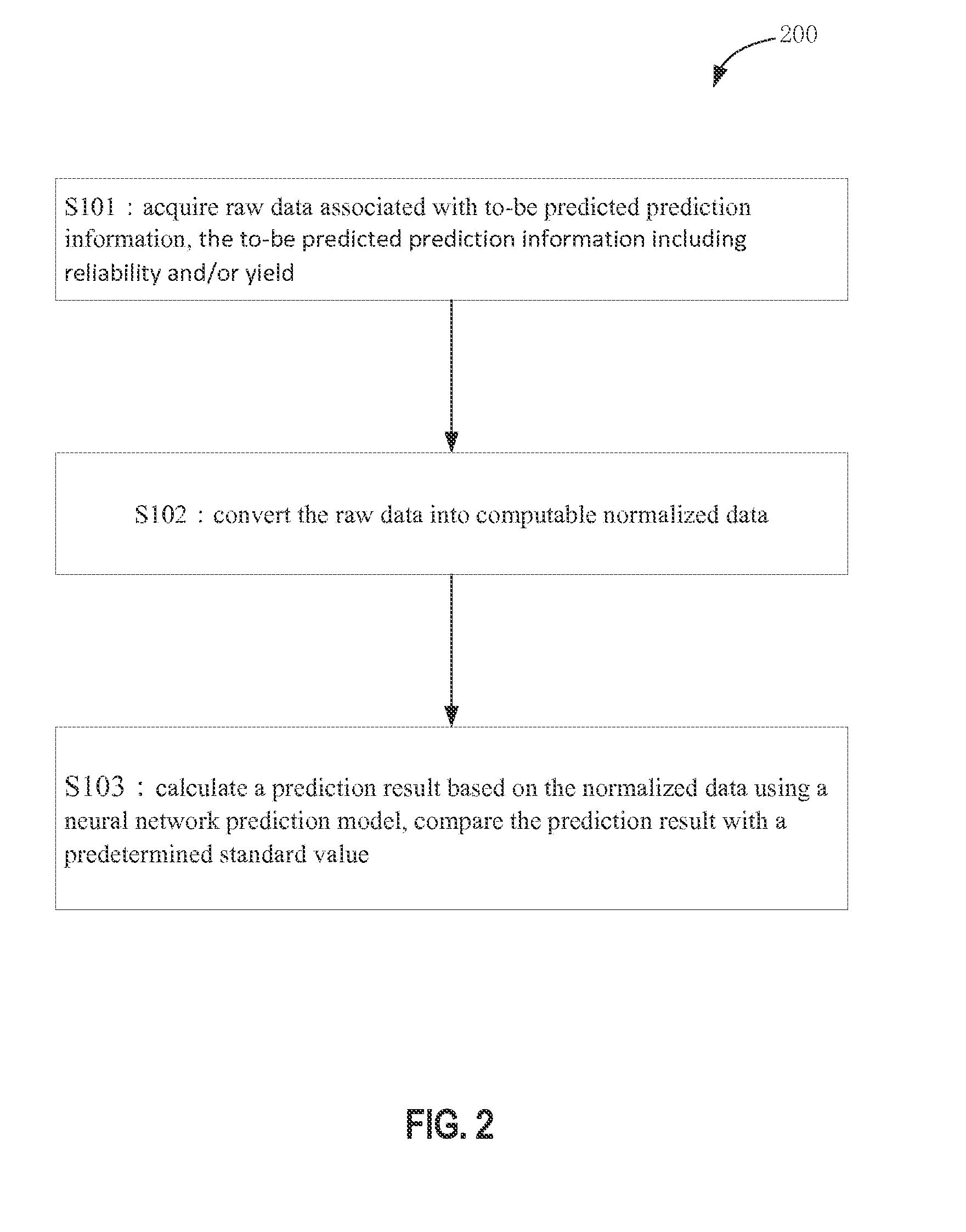
[0076]Embodiments of the present invention provide a method for predicting product information in a semiconductor device manufacturing process that is performed using the above-described prediction system. The predicting method for product information in a semiconductor device manufacturing process may prevent major reliability and / or yield problems through inline data acquisition and the computed prediction result of the to-be predicted prediction information (reliability or yield). The prediction result of the to-be predicted prediction information (reliability or yield) is computed using a neural network prediction model.

[0077]FIG. 2 is a simplified flow chart of a method 200 for predicting information of a semiconductor device according to one embodiment of the present invention. FIG. 3 is a simplified flow chart of a method 300 for predicting information of a semiconductor device according to another embodiment of the present invention

[0078]Referring to FIGS. 1 and 2, the metho...


PUM


Abstract

A system and method for predicting a product characteristic are provided. The system includes a data acquisition module configured to acquire raw data associated with to-be predicted prediction information, a data conversion module configured to convert the raw data into computable normalized data, and a result prediction module configured to calculate a prediction result based on the normalized data and compare the prediction result with a predetermined standard value. The result prediction module includes a neural network prediction model configured to calculate the prediction result based on the normalized data. The prediction information may include reliability and/or yield to prevent major reliability or yield problems from occurring during manufacturing of semiconductor devices.

Description

CROSS-REFERENCES TO RELATED APPLICATIONS[0001]This application claims priority to Chinese patent application No. 201410276855.7, entitled “PREDICTING CIRCUIT RELIABILITY AND YIELD USING NEURAL NETWORKS” filed Jun. 19, 2014, the content of which is incorporated herein by reference in its entirety.BACKGROUND OF THE INVENTION[0002]The present invention relates generally to semiconductor device manufacturing, and more particularly to a system and method for predicting reliability and yield of a semiconductor device.[0003]Yield and reliability are two important factors that may affect the development and profitability of semiconductor device manufacturing. Traditionally, semiconductor device reliability has been estimated from accelerated stress tests after the completion of manufactured semiconductor devices. Similarly, yield may be obtained from wafer test results after the completion of the manufactured semiconductor device. Because wafer yield and reliability risk are critical parame...

Claims


Application Information

Patent Timeline
Patent Type & Authority Applications(United States)
IPC IPC(8): G06N3/08
CPCG06N3/08G05B19/41875G05B23/0294G06N3/02G06Q10/0639G06F30/39Y02P90/02
Inventor CHIEN, WEITINGSII, HOWKINGKANG, SHENG
Owner SEMICON MFG INT (SHANGHAI) CORP
Why Eureka
Try Eureka