Buckled organic light emitting diode for light extraction without blurring

Active Publication Date: 2015-12-24
UNIV OF FLORIDA RES FOUNDATION INC
View PDF7 Cites 0 Cited by
  • Summary
  • Abstract
  • Description
  • Claims
  • Application Information

AI Technical Summary

Benefits of technology

[0006]Other embodiments of the invention are directed to methods of preparing an OLED device that comprise steps to deposit a transparent elastomeric layer on a transparent substrate; depositing a metal layer of 5 to 100 nm on a portion of the transparent elastomeric layer, where

Problems solved by technology

Organic light emitting diodes (OLEDs) suffer from a relatively low efficiency of emitted light relative to that generated because of light trapping due to a refractive index mismatch between the air (n=1), glass substrate (n=1.52), and an electrode/active layer, for example, an ITO/organi

Method used


Image

  • Buckled organic light emitting diode for light extraction without blurring
  • Buckled organic light emitting diode for light extraction without blurring
  • Buckled organic light emitting diode for light extraction without blurring

Examples


Example

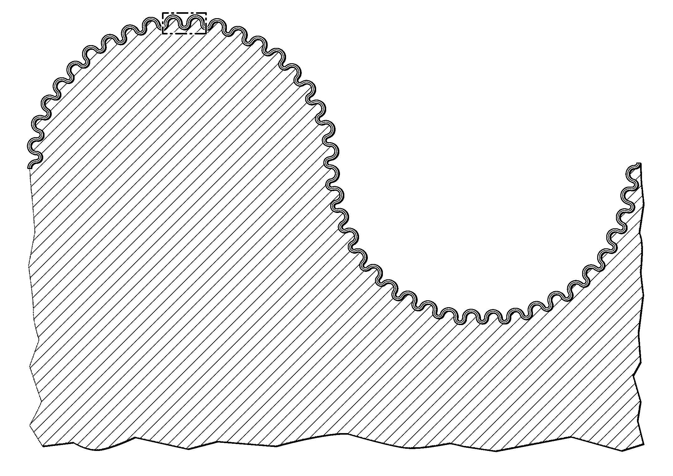
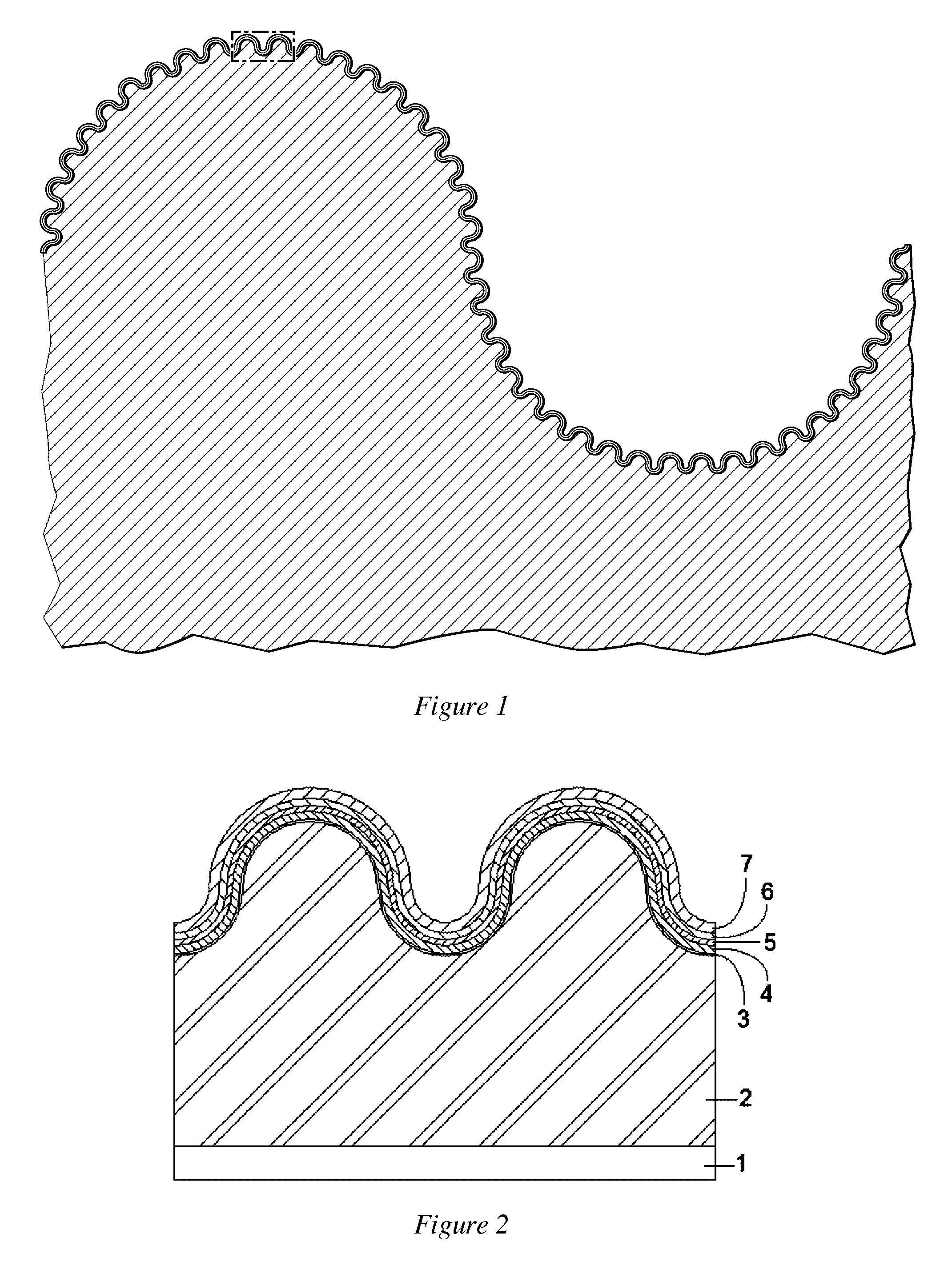
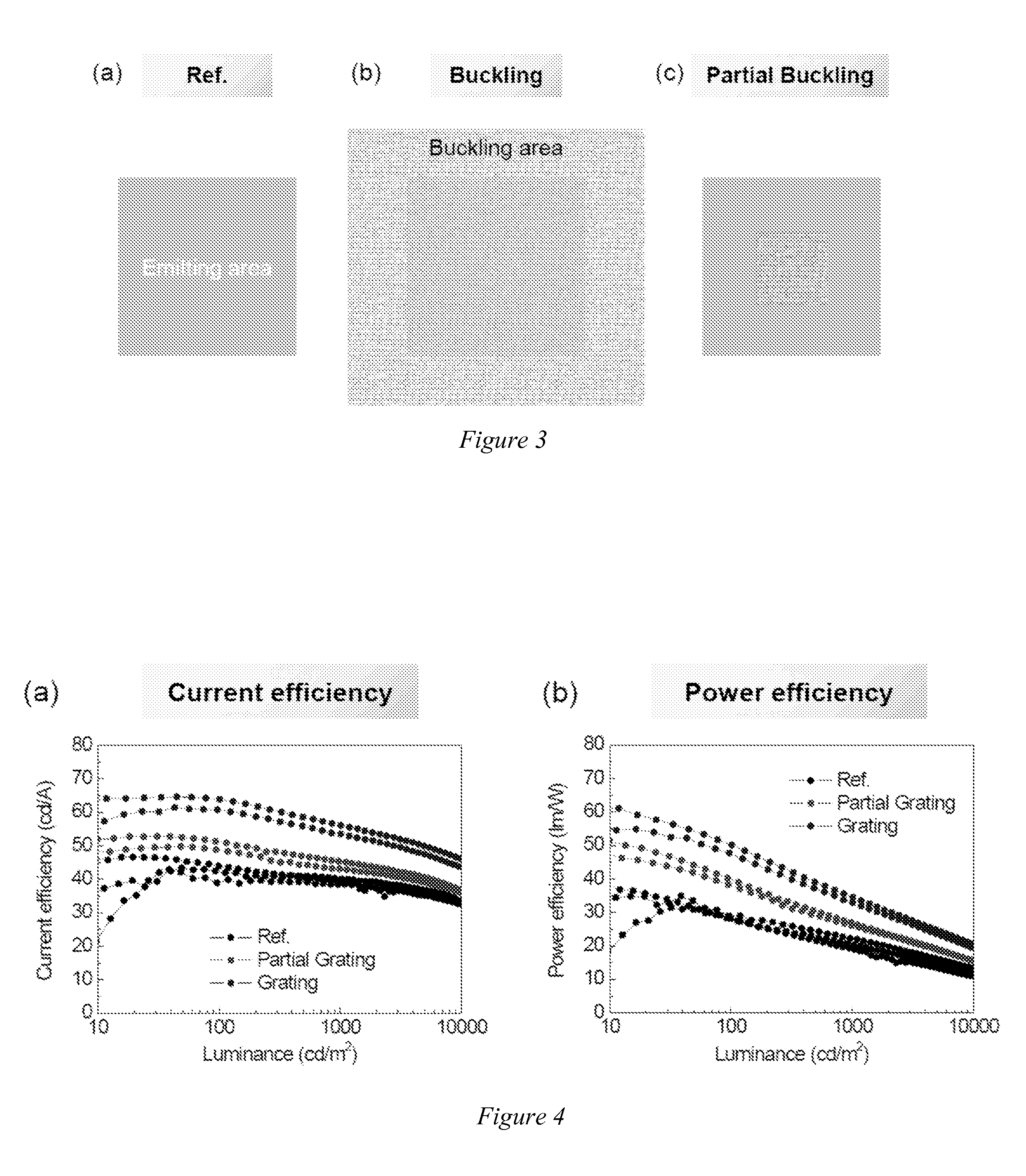
[0012]Embodiments of the invention are directed to an organic light emitting diode (OLED) comprising a quasi-periodic grating that has a buckling structure that occupies a portion of the emitting area that is less than the entire emitting area. In an embodiment of the invention, the buckling comprises a fine buckling upon a gross buckling. The buckling is on a surface distal to the light exiting face where a transparent elastomer layer is adjacent to a transparent substrate at the light exiting face of the OLED. The buckled structure does not cover the entire area of the OLED light emitting area, where the outer portions of the light emitting area do not have a buckling topography on the distal face. The fine buckling structure is of dimensions that extract the waveguide modes of the OLED and have periodicities or quasi-periodicities of about 100 to about 700 nm. The gross buckling has a periodicity or quasi-periodicities of about 10 to 20 μm. The quasi-periodic buckling, of approxi...


PUM


Abstract

A layered organic light emitting diode (OLED) device comprises a buckled structure over a portion of the light emitting face to provide improved light output relative to flat OLED devices. The buckled structure has a fine buckling and a gross buckling, which are quasi-periodic. Embodiments of the invention are directed to a method of producing the OLED device comprising a buckled structure, where a transparent substrate coated with a transparent elastomeric layer has a thin metal layer deposited on a portion of the elastomeric layer at an elevated temperature. Upon cooling the metal layer buckles with the formation of the quasi-periodic buckling. Subsequently the metal layer is oxidized to a metal oxide layer that retains the buckling. An OLED with a buckling structure over a portion of the emitting face is constructed on the metal oxide layer and retains the buckling of the metal oxide layer.

Description

BACKGROUND OF INVENTION[0001]Organic light emitting diodes (OLEDs) suffer from a relatively low efficiency of emitted light relative to that generated because of light trapping due to a refractive index mismatch between the air (n=1), glass substrate (n=1.52), and an electrode / active layer, for example, an ITO / organic layer (˜1.7 to ˜2.0) in waveguide modes. The imposition of a periodic microstructure into an OLED permits the recovery of a portion of the lost light. Unfortunately, although improvement of the light output has occurred, the cost to achieve the periodic microstructure is that of complicating the process with lithographic and imprinting steps to prepare and transfer the microstructure to the OLED.[0002]Bowden et al., Nature 1998, 393, 146-9 demonstrated the preparation of buckled structure by the deposition of metal films on a thermally expanded 1 cm thick polydimethylsiloxane (PDMS) rubber film, where upon subsequent cooling of the films, buckling of the metal film res...

Claims


Application Information

Patent Timeline
IPC IPC(8): H01L51/52H01L51/00H01L51/56H01L51/50
CPCH01L51/5209H01L51/5225H01L51/5275H01L51/0096H01L51/56H01L51/5056H01L51/5215H01L51/5221H01L51/5012Y02E10/549H10K50/813H10K50/822H10K50/858H10K50/11H10K50/816H10K71/00H10K77/10H10K50/15H10K50/82
Inventor SO, FRANKYKOO, WONHOE
Owner UNIV OF FLORIDA RES FOUNDATION INC
Why Eureka
Try Eureka