Printed circuit board, package substrate, and method of fabricating the same

a technology of printed circuit board and package substrate, which is applied in the direction of printed circuit non-printed electric components association, electrical apparatus construction details, and semiconductor/solid-state device details, etc. it can solve problems such as solder cracks, solder bridges, solder collapses, etc., and achieve fine pitch and enhanced degree of freedom , the effect of maximizing the productivity of the manufacturer

Active Publication Date: 2015-12-31
LG INNOTEK CO LTD
View PDF4 Cites 42 Cited by
  • Summary
  • Abstract
  • Description
  • Claims
  • Application Information

AI Technical Summary

Benefits of technology

[0018]The embodiment provides a printed circuit board in which a fine pitch can be easily formed.
[0041]As described above, according to the embodiment, the bump is formed on the lower substrate, and the upper substrate is attached to the lower substrate using the bump, thereby fabricating the package substrate, so that the fine pitch can be formed. Accordingly, the productivity of a manufacturer can be maximized.
[0042]In addition, according to the embodiment, the electronic device exposed to the outside is attached on the lower substrate and the attachment space of the electronic device is molded using resin in the package process performed together with the upper substrate. Accordingly, the degree of freedom can be enhanced in the design of the substrate for the attachment of the electronic device, and the productivity can be improved in terms of product yield.
[0043]In addition, according to the embodiment, since the molding area formed between the lower substrate and the upper substrate is supported by the metal post formed on the lower substrate, the electronic device attached to the molding area can be efficiently protected, so that the reliability of the package substrate can be improved.
[0044]Further, according to the embodiment, the lateral side of the metal post is curved and the metal post has the shape of a trapezoid having the upper width narrower than the lower width, so that the distance between adjacent metal posts is increased to prevent the short failure. In addition, the upper substrate can be attached to the lower substrate using a small amount of solder.
[0045]In addition, according to the embodiment, since the metal post is formed through an etch scheme instead of a pattern plating scheme, the fabrication cost of the printed circuit board can be reduced.

Problems solved by technology

However, the related art has a limitation in forming a fine pitch since the first substrate is connected with the second substrate using the solder ball 7.
In addition, according to the related art, since the solder ball 7 is used, issues such as a solder crack, a solder bridge, and a solder collapse, may be occur.

Method used


Image

  • Printed circuit board, package substrate, and method of fabricating the same
  • Printed circuit board, package substrate, and method of fabricating the same
  • Printed circuit board, package substrate, and method of fabricating the same

Examples


Embodiment Construction

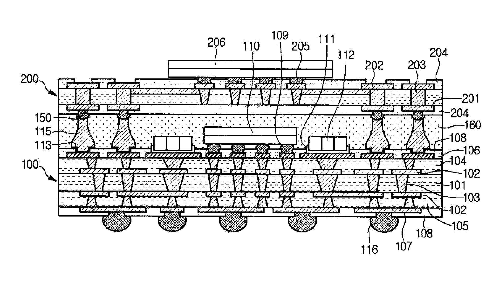
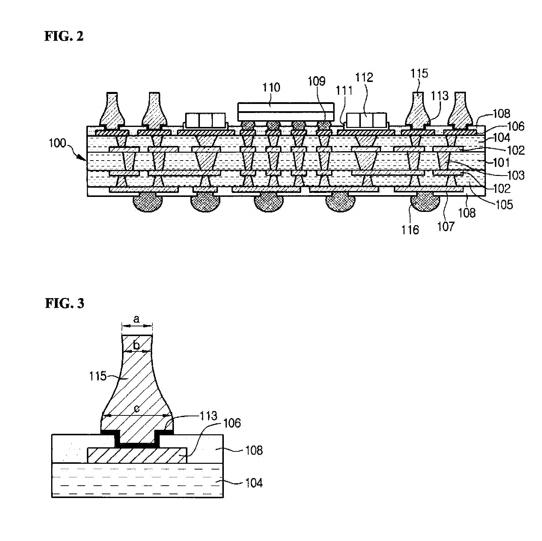
[0053]Hereinafter, embodiments will be described in detail with reference to accompanying drawings so that those skilled in the art can easily work with the embodiments. However, the embodiments may have various modifications.

[0054]In the following description, when a predetermined part “includes” a predetermined component, the predetermined part does not exclude other components, but may further include other components unless indicated otherwise.

[0055]The thickness and size of each layer shown in the drawings may be exaggerated, omitted or schematically drawn for the purpose of convenience or clarity. In addition, the size of elements does not utterly reflect an actual size. The same reference numbers will be assigned the same elements throughout the drawings.

[0056]In the description of the embodiments, it will be understood that, when a layer (or film), a region, or a plate is referred to as being “on” another part, it can be “directly” or “indirectly” over the other part, or one...


PUM


Abstract

A printed circuit board includes an insulating substrate, a plurality of pads on a top surface of the insulating substrate, a protective layer formed on the insulating substrate and having an opening to expose top surfaces of the pads, a bump formed on at least one of the pads and protruding upward of a surface of the protective layer. The bump has a curved lateral side.

Description

CROSS-REFERENCE TO RELATED APPLICATIONS[0001]The present application claims priority under 35 U.S.C. §119 to Korean Patent Application No. 10-2014-0080822, filed Jun. 30, 2014, which is hereby incorporated by reference in its entirety.BACKGROUND[0002]1. Field of the Invention[0003]The embodiment relates to a printed circuit board, a package substrate, and a method of fabricating the same.[0004]2. Description of Related Art[0005]In general, the package substrate has a structure in which a first substrate having a memory chip attached thereto is integrated with a second substrate having a processor chip attached thereto.[0006]The package substrate has advantages in that the mounting area of the chips can be reduced, and a signal can be transmitted at a high rate as the processor chip and the memory chip are integrated in one package.[0007]The package substrate has been extensively applied to various mobile appliances due to the advantages.[0008]FIG. 1 is a sectional view showing a pac...

Claims


Application Information

Patent Timeline
Patent Type & Authority Applications(United States)
IPC IPC(8): H05K1/11H05K3/34H05K1/18
CPCH01L23/49822H01L2924/19043H05K3/4007H05K2201/0367H05K2201/042H05K2203/1383H01L2924/181H01L2924/15311H01L2924/19105H05K1/144H01L2924/19042H01L2924/19041H01L2924/15331H01L2924/1434H01L25/105H01L24/13H01L24/16H01L24/81H01L25/50H01L2224/131H01L2224/16227H01L2224/81192H01L2225/1023H01L2225/1058H01L2924/00012H01L2924/014H01L2924/00014H01L21/486H01L23/49827H05K1/111
Inventor KIM, DONG SUNRYU, SUNG WUKSEO, HYUN SEOKLEE, JI HAENG
Owner LG INNOTEK CO LTD
Why Eureka
Try Eureka