Semiconductor package and method of manufacturing the same

Inactive Publication Date: 2016-01-07
SAMSUNG ELECTRONICS CO LTD
View PDF5 Cites 20 Cited by
  • Summary
  • Abstract
  • Description
  • Claims
  • Application Information

AI Technical Summary

Benefits of technology

[0029]According to some additional embodiments, a plurality of gap adjusting bumps may be arranged on the package board along the peripheral portion of the semiconductor chip, and thus the semiconductor chip may be spaced apart from the chip board at a minimal gap distance corresponding to the height of the gap adjustin

Problems solved by technology

Unfortunately, applying compression to ensure adequate contact and connection may also cause a smaller gap space than desired.
Insufficient flow of under-fill materials may be a direct result.
This results in voids w

Method used


Image

  • Semiconductor package and method of manufacturing the same
  • Semiconductor package and method of manufacturing the same
  • Semiconductor package and method of manufacturing the same

Examples


Example

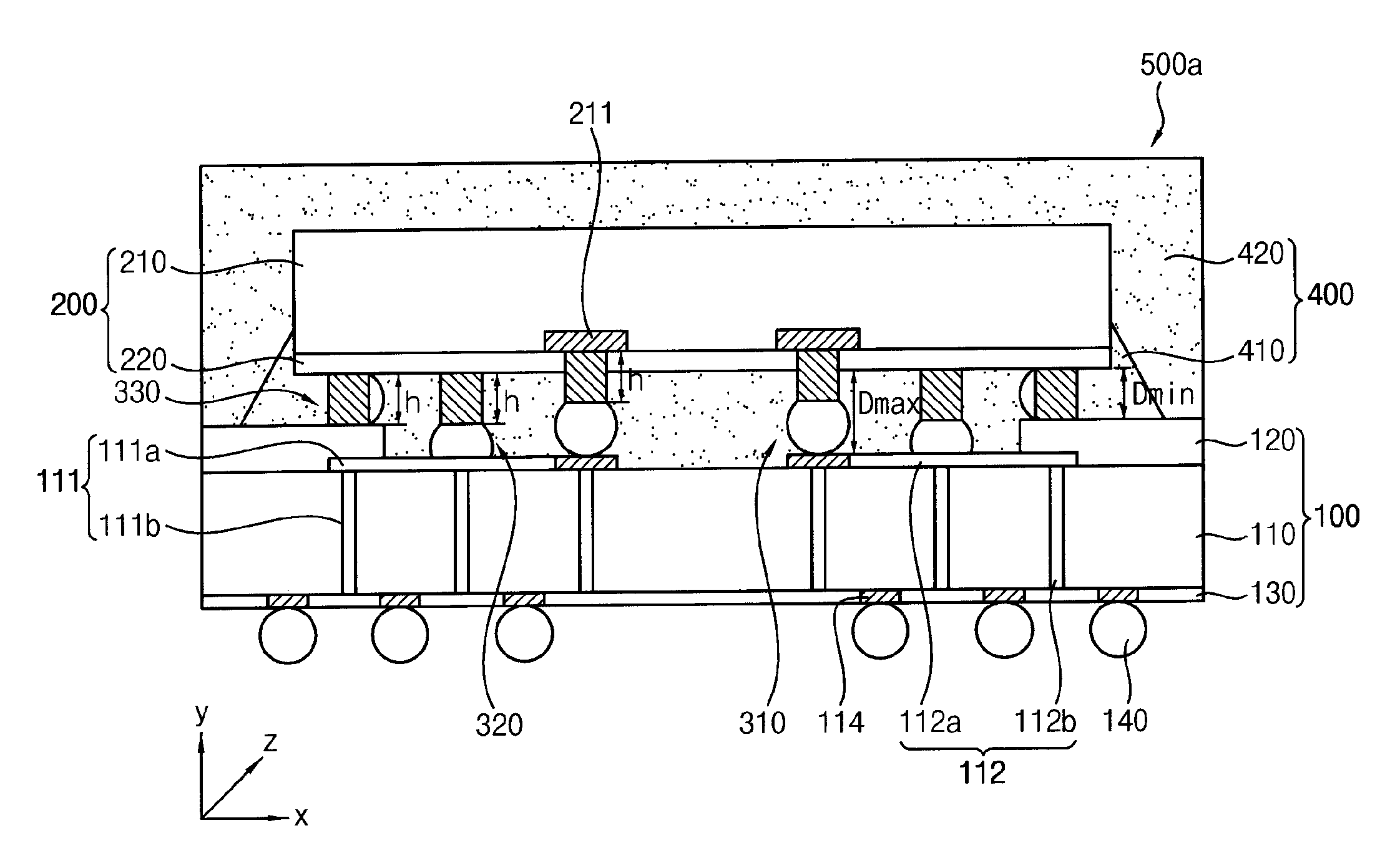
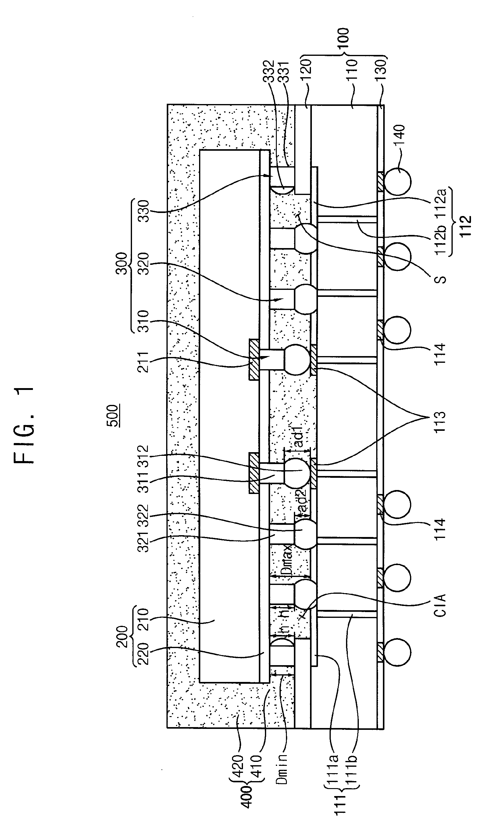
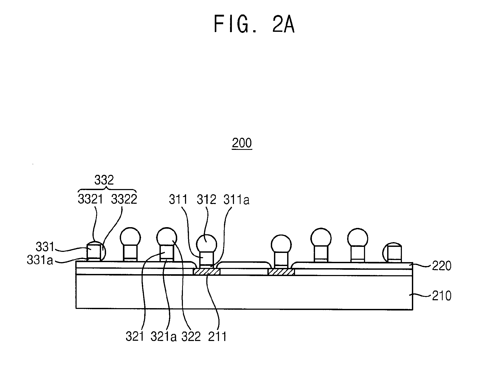
[0042]Various exemplary embodiments will be described more fully hereinafter with reference to the accompanying drawings. The teachings herein may, however, be embodied in many different forms and should not be construed as limited to the embodiments set forth herein. Rather, embodiments disclosed herein are introductory, and will merely introduce concepts to those skilled in the art. In the drawings, the sizes and relative sizes of layers and regions may be exaggerated for clarity.

[0043]As discussed herein, the term “exemplary” is not meant to imply a superlative. Rather, the term “exemplary” merely refers to one of many possible embodiments.

[0044]It will be understood that when an element is referred to as being “on,”“connected to” or “coupled to” another element, the first element can be directly on, connected or coupled to the other element. Other intervening elements may be present. In contrast, when an element is referred to as being “directly on,”“directly connected to” or “d...


PUM


Abstract

A semiconductor package includes a package board that includes an circuit pattern and a plurality of contact pads electrically connected to the circuit pattern; a semiconductor chip having a plurality of chip pads; and a bump structure including a plurality of connecting bumps electrically connected with the semiconductor chip and the circuit pattern and a plurality of gap adjusting bumps bonded to the semiconductor chip and shaped into a slender bar between the semiconductor chip and the package board, the gap adjusting bumps spacing the semiconductor chip from the package board such that a gap space, S, is maintained between the package board and the semiconductor chip. A method of fabrication and a memory unit are disclosed.

Description

CROSS-REFERENCE TO RELATED APPLICATIONS[0001]This application claims priority under 35 U.S.C. §119 to Korean Patent Application No. 10-2014-0082448 filed on Jul. 2, 2014 in the Korean Intellectual Property Office, the disclosure of which is incorporated by reference herein in its entirety.BACKGROUND[0002]1. Field[0003]Example embodiments relate to a semiconductor package and method of manufacturing the same, and more particularly, to a flip chip package and a method of manufacturing the flip chip package.[0004]2. Description of the Related Art[0005]The continuing demand for high performance electronics has brought about development of many improvements to packaging of semiconductor circuitry. In particular, a flip-chip package has been widely used in the semiconductor industry due to small size of the semiconductor package.[0006]In conventional flip-chip packages, a plurality of bumps arranged on an active face of the semiconductor chip provide electrical contacts for access to the ...

Claims


Application Information

Patent Timeline
IPC IPC(8): H01L23/00
CPCH01L24/17H01L24/81H01L2924/1436H01L2224/1712H01L2924/014H01L24/11H01L24/14H01L2224/16145H01L2224/16225H01L2924/15311H01L2924/181H01L24/16H01L24/29H01L24/32H01L24/92H01L2224/13101H01L2224/13124H01L2224/13147H01L2224/1412H01L2224/2919H01L2224/32225H01L2224/73204H01L2224/81815H01L2224/92125H01L2225/06513H01L23/49816H01L23/49827H01L23/16H01L23/3128H01L25/0657H01L2225/06517H01L2225/06541H01L2924/00012H01L2924/0665H01L2924/00
Inventor KWON, YONG-HWANPARK, MYEONG-SOONLEE, CHAN-HO
Owner SAMSUNG ELECTRONICS CO LTD
Why Eureka
Try Eureka