Organic light emitting display device and manufacturing method thereof

a technology of light-emitting display device and organic material, which is applied in the direction of thermoelectric device, organic semiconductor device, semiconductor/solid-state device details, etc., can solve the problems of high resistance of cathodes, aggravate voltage drop problems, and non-uniform luminance or image quality, so as to prevent voltage drop of cathodes and simplify the process

Active Publication Date: 2016-01-14
LG DISPLAY CO LTD
View PDF4 Cites 62 Cited by
  • Summary
  • Abstract
  • Description
  • Claims
  • Application Information

AI Technical Summary

Benefits of technology

[0021]Therefore, an aspect of the detailed description is to provide a top emission type organic light emitting display device in which a voltage drop of a cathode is prevented, while simplifying a process, and a manufacturing method thereof.
[0022]Another aspect of the detailed description is to provide an organic light emitting display device in which voltage drop of a cathode is prevented, while enhancing reliability of contact between a cathode and an auxiliary electrode, and a manufacturing method thereof.
[0043]According to the organic light emitting display device and a manufacturing method thereof of embodiments of the present disclosure, an auxiliary electrode having a multilayer structure including different kinds of metals different in etching speed is formed, and when an anode is formed, a void is formed within the auxiliary electrode such that the auxiliary electrode is in direct contact with a cathode. Thus, resistance of the cathode may be reduced, while the process is simplified.
[0044]According to the organic light emitting display device and a manufacturing method thereof of embodiments of the present disclosure, defects may be reduced to enhance productivity, and luminance uniformity and reliability of the organic light emitting display device may be enhanced.

Problems solved by technology

However, doing so causes the cathode to have high resistance.
Thus, voltages having different levels are applied to subpixels, causing non-uniformity of luminance or image quality.
In particular, as the size of a display panel increases, the voltage drop problem may be aggravated.

Method used


Image

  • Organic light emitting display device and manufacturing method thereof
  • Organic light emitting display device and manufacturing method thereof
  • Organic light emitting display device and manufacturing method thereof

Examples


first embodiment

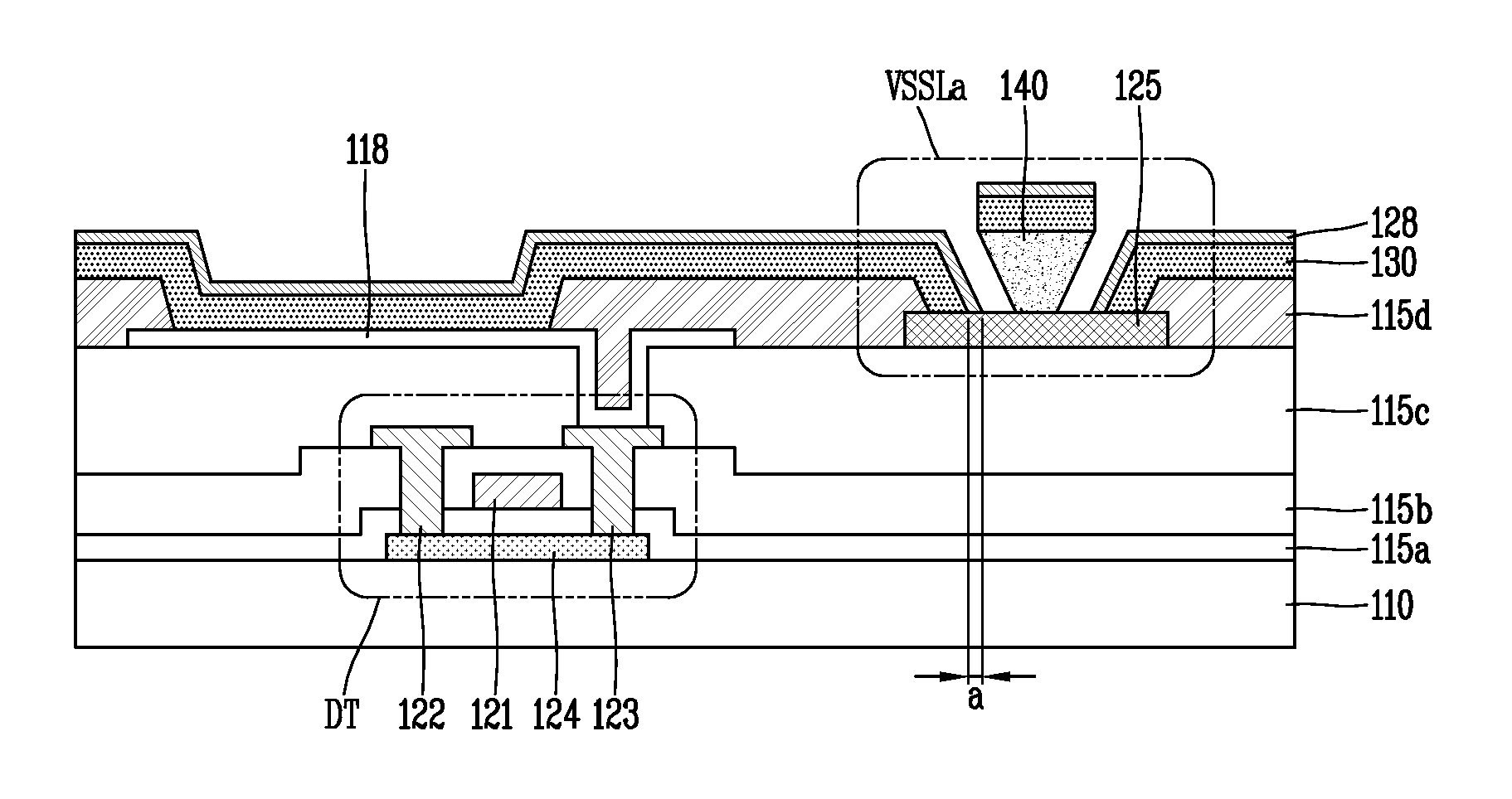
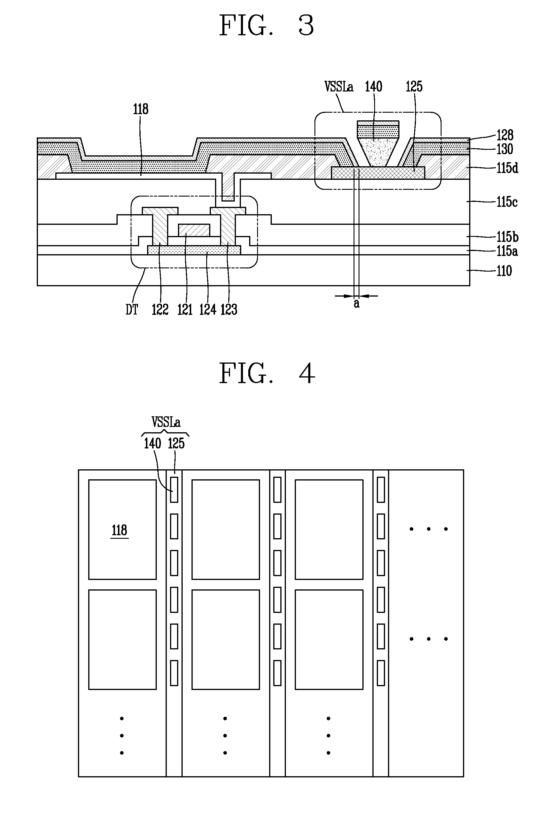
[0089]Here, in the present disclosure, the bank 115d may further include a second opening exposing a portion of an auxiliary electrode 125 (to be described hereinafter).

[0090]The organic compound layer 130 is formed between the first electrode and the second electrode 128. The organic compound layer 130 emits light according to combination of holes supplied from the first electrode 118 and electrons supplied from the second electrode 128.

[0091]Here, in FIG. 3, it is illustrated that the organic compound layer 130 is formed on the entire surface of the substrate 110, but the present disclosure is not limited thereto. The organic compound layer 130 may be formed only on the first electrode 118.

[0092]The organic compound layer 130 may have a multilayer structure including an auxiliary layer for enhancing luminous efficiency of the emission layer, in addition to the emission layer emitting light.

[0093]The second electrode 128 is formed on the organic compound layer 130 to provide electr...

second embodiment

[0106]FIG. 5 is a cross-sectional view schematically illustrating a portion of a structure of an organic light emitting display device according to the present disclosure.

[0107]Here, FIG. 5 illustrates a top emission type organic light emitting display device using a TFT having a coplanar structure. However, the present disclosure is not limited to the TFT having a coplanar structure.

[0108]Referring to FIG. 5, the top emission type organic light emitting display device according to the second embodiment may include a substrate 210, a driving TFT DT, an OLED, and an auxiliary electrode line VSSLa.

[0109]Like that of the first embodiment described above, the driving TFT DT according to the second embodiment includes a semiconductor layer 224, a gate electrode 221, a source electrode 222, and a drain electrode 223.

[0110]The semiconductor layer 224 is formed on the substrate 210 formed of an insulating material such as transparent plastic or a polymer film.

[0111]The semiconductor layer 2...

third embodiment

[0211]FIG. 8 is a cross-sectional view schematically illustrating a portion of a structure of an organic light emitting display device according to the present disclosure.

[0212]Here, the organic light emitting display device according to a third embodiment of the present disclosure illustrated in FIG. 8 has the substantially same configuration as that of the organic light emitting display device according to the second embodiment of the present disclosure described above, except that voids are formed on both sides of an auxiliary electrode and a connection electrode is patterned to have the substantially same shape as that of the first substrate.

[0213]FIG. 8 shows a top emission type organic light emitting display device using a TFT having a coplanar structure, as an example. However, the present disclosure is not limited thereto.

[0214]Referring to FIG. 8, the top emission type organic light emitting display device according to the third embodiment of the present disclosure may incl...


PUM


Abstract

Provided are an organic light emitting display device and a manufacturing method thereof. In the organic light emitting display device, after an auxiliary electrode having a multilayer structure including different kinds of metals different in etching speed is formed, a void is formed within the auxiliary electrode upon formation of an anode. The resulting structure is created by a simplified process, with contact reliability between a cathode and the auxiliary electrode being enhanced, while resistance of the cathode is reduced.

Description

CROSS-REFERENCE TO RELATED APPLICATION[0001]Pursuant to 35 U.S.C. §119(a), this application claims the benefit of earlier filing date and right of priority to Korean Applications No. 10-2014-0085414, filed on Jul. 8, 2014, and No. 10-2015-0090667, filed on Jun. 25, 2015, the contents of which are incorporated by reference herein in its entirety.BACKGROUND OF THE INVENTION[0002]1. Field of the Invention[0003]The present disclosure relates to an organic light emitting display device and a manufacturing method thereof, and particularly, to a top emission type organic light emitting display device and a manufacturing method thereof.[0004]2. Background of the Invention[0005]Recently, interest in information displays has been on the rise, demand for using portable information mediums has grown, and research into and commercialization of lighter, thinner flat panel displays (FPDs) has actively conducted.[0006]In the flat panel display field, liquid crystal displays (LCDs) which are light i...

Claims


Application Information

Patent Timeline
Patent Type & Authority Applications(United States)
IPC IPC(8): H01L51/52H01L51/56
CPCH01L51/5228H01L51/5206H01L2251/308H01L2251/301H01L51/56H10K59/1315H10K59/122H10K59/80517H10K59/80516H10K59/80523H10K59/873H10K59/80522H10K59/80524H10K59/1213H10K59/124H01L29/7869H10K59/123H10K59/82H10K59/8792H10K2102/103H10K2102/3026H10K50/824H10K50/81H10K71/00H10K50/814H10K2102/00
Inventor IM, JONGHYEOKKIM, SEJUNELEE, JOONSUKLEE, SOJUNGLEE, JAESUNG
Owner LG DISPLAY CO LTD
Why Eureka
Try Eureka