Method and system for logic built-in self-test

a logic and built-in technology, applied in the direction of electronic circuit testing, measurement devices, instruments, etc., can solve the problems of exceeding tolerable levels, unreasonably high electrical power generated during full-chip lbist scan, and time-consuming scan tests

Active Publication Date: 2016-01-28
NXP USA INC
View PDF6 Cites 13 Cited by
  • Summary
  • Abstract
  • Description
  • Claims
  • Application Information

AI Technical Summary

Problems solved by technology

This test cycle is typically repeated many times, which, given the size of integrated circuits today, makes scan test time consuming.
However, the electrical power generated during a full-chip LBIST scan can become unreasonably high, sometimes exceeding tolerable levels.
Shift speeds and therefore LBIST run time are limited by the current consumption of the device under test.
Another problem associated with LBIST testing, particularly at start-up, is the creation of a large voltage drop, which can lead to failures.

Method used


Image

  • Method and system for logic built-in self-test
  • Method and system for logic built-in self-test

Examples


Embodiment Construction

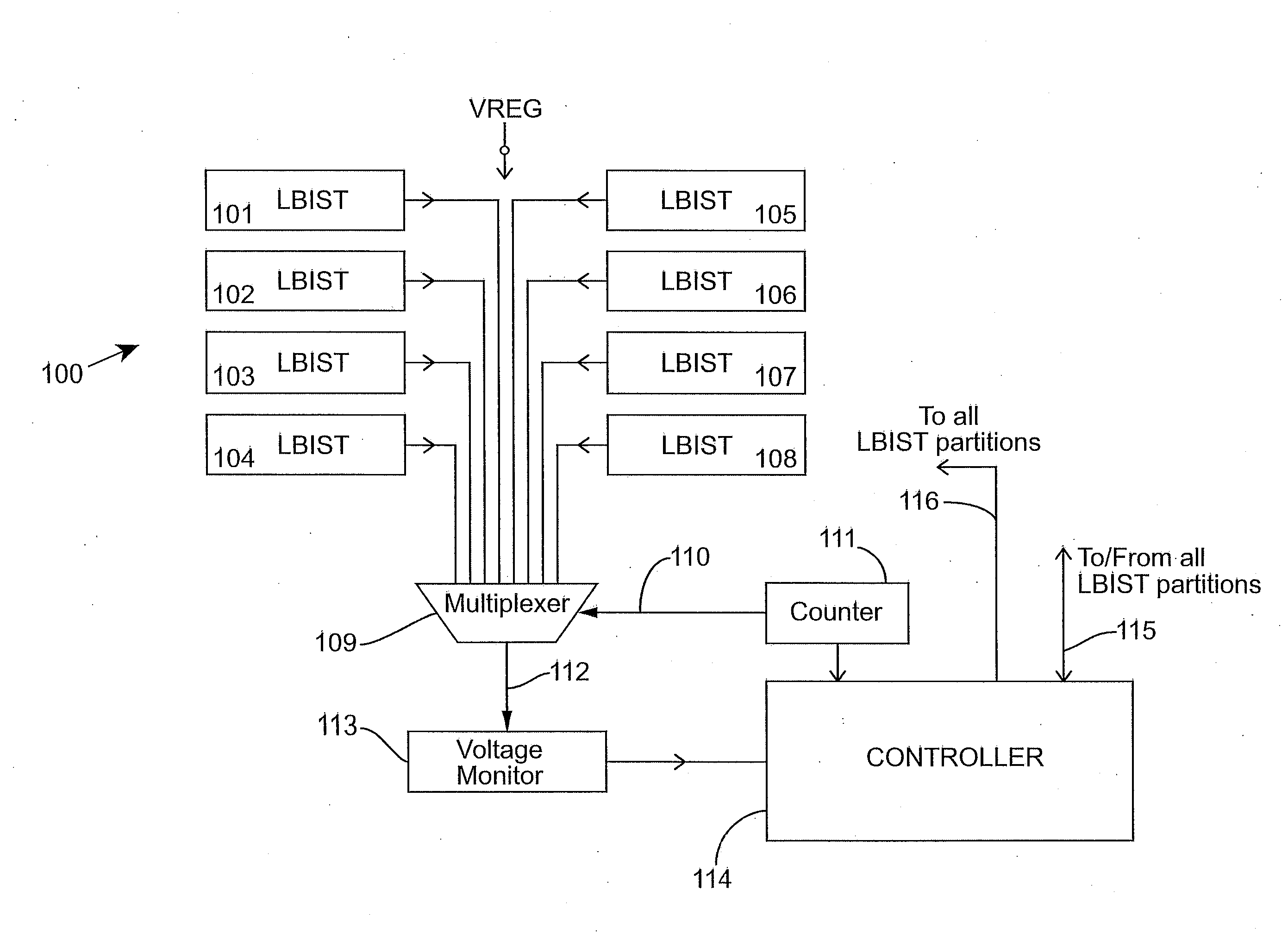
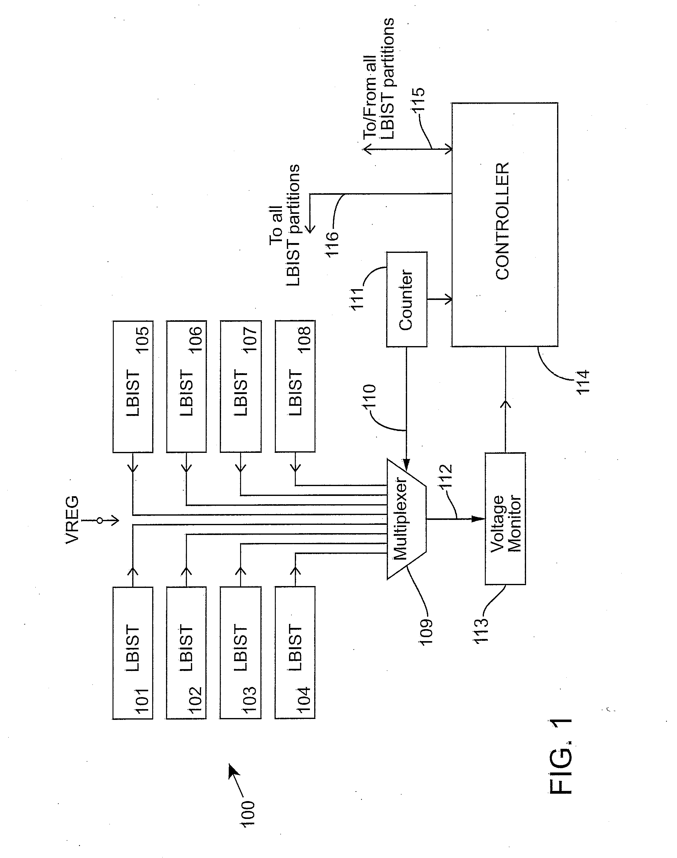
[0007]The detailed description set forth below in connection with the appended drawings is intended as a description of presently preferred embodiments of the invention, and is not intended to represent the only forms in which the present invention may be practiced. It is to be understood that the same or equivalent functions may be accomplished by different embodiments that are intended to be encompassed within the spirit and scope of the invention. In the drawings, like numerals are used to indicate like elements throughout. Furthermore, terms “comprises,”“comprising,” or any other variation thereof, are intended to cover a non-exclusive inclusion, such that module, circuit, device components, structures and method steps that comprises a list of elements or steps does not include only those elements but may include other elements or steps not expressly listed or inherent to such module, circuit, device components or steps. An element or step proceeded by “comprises_a” does not, wi...


PUM


Abstract

A controller executes a first LBIST test on a device at a first shift frequency on a plurality of partitions and detects any voltage drop at sense points in each partition during the test. If a voltage drop is detected, then the test is re-run for those partitions that failed the first test. If failures are detected during the re-execution, then a further test at a lower shift frequency is performed. The partitions can be tested sequentially or in parallel and invention has the advantage of reducing the time taken for executing LBIST when the device is booted.

Description

BACKGROUND OF THE INVENTION[0001]The present invention relates generally to integrated circuits and testing integrated circuits and, more particularly, to a method and system for testing an integrated circuit using Logic Built-in Self-test (LBIST).[0002]Integrated circuits, such as microprocessors or system-on-chip (SOC) devices typically include a complex matrix of logic gates arranged to perform particular functions. These logic gates are often interconnected in two parallel arrangements, one for operation, and another for testing circuit functionality. Linking a plurality of latches together into a “scan chain” is one known method of arranging logic gates for testing. Such scan chains may be used to gain access to internal nodes of the integrated circuit. Test patterns are shifted in by the scan chains and functional clock signals are pulsed to test the circuit during a capture cycle. The results are then shifted to output pins and compared against expected results. This test cyc...

Claims


Application Information

Patent Timeline
Patent Type & Authority Applications(United States)
IPC IPC(8): G01R31/3177
CPCG01R31/3177G01R31/3187G01R31/31724
Inventor SINGH, NITINJINDAL, AMITJINDAL, ANURAG
Owner NXP USA INC
Why Eureka
Try Eureka