Semiconductor optical device
a technology of semiconductors and optical devices, applied in the field of semiconductor optical devices, can solve the problems of incompatibility of active devices and active devices with cladding layers, and achieve the effect of good compatibility
- Summary
- Abstract
- Description
- Claims
- Application Information
AI Technical Summary
Benefits of technology
Problems solved by technology
Method used
Image

Examples
first embodiment
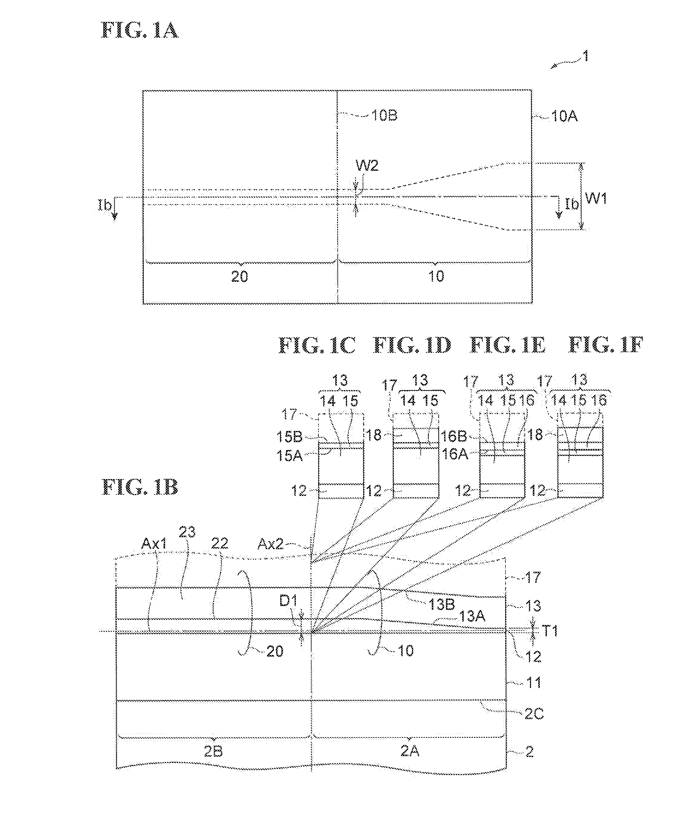
[0025]FIGS. 1A to 1F are views illustrating a structure of a semiconductor optical device according to a first embodiment. FIG. 1A is a plan view that schematically illustrates the semiconductor optical device. FIG. 1B is a cross-sectional view taken along line 1b-1b in FIG. 1A. FIGS. 1C to 1F are views illustrating typical structural examples of FIG. 1B.
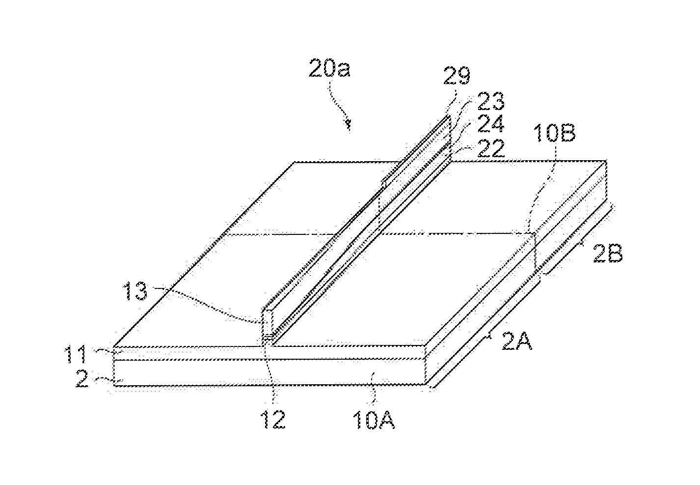
[0026]Referring to FIGS. 1A and 1B, a semiconductor optical device 1 according to the first embodiment includes a first semiconductor optical waveguide 10 and a second semiconductor optical waveguide 20. The first optical waveguide 10 is disposed on a first region 2A of a substrate 2. The second optical waveguide 20 is disposed on a second region 2B on the substrate 2. The first and second optical waveguides 10 and 20 extend along a first direction Ax1. The first optical waveguide 10 is optically coupled with the second optical waveguide 20 at a boundary 10B between the first region 2A and the second region 2B. The first optical wav...
example 3
Structural Example 3
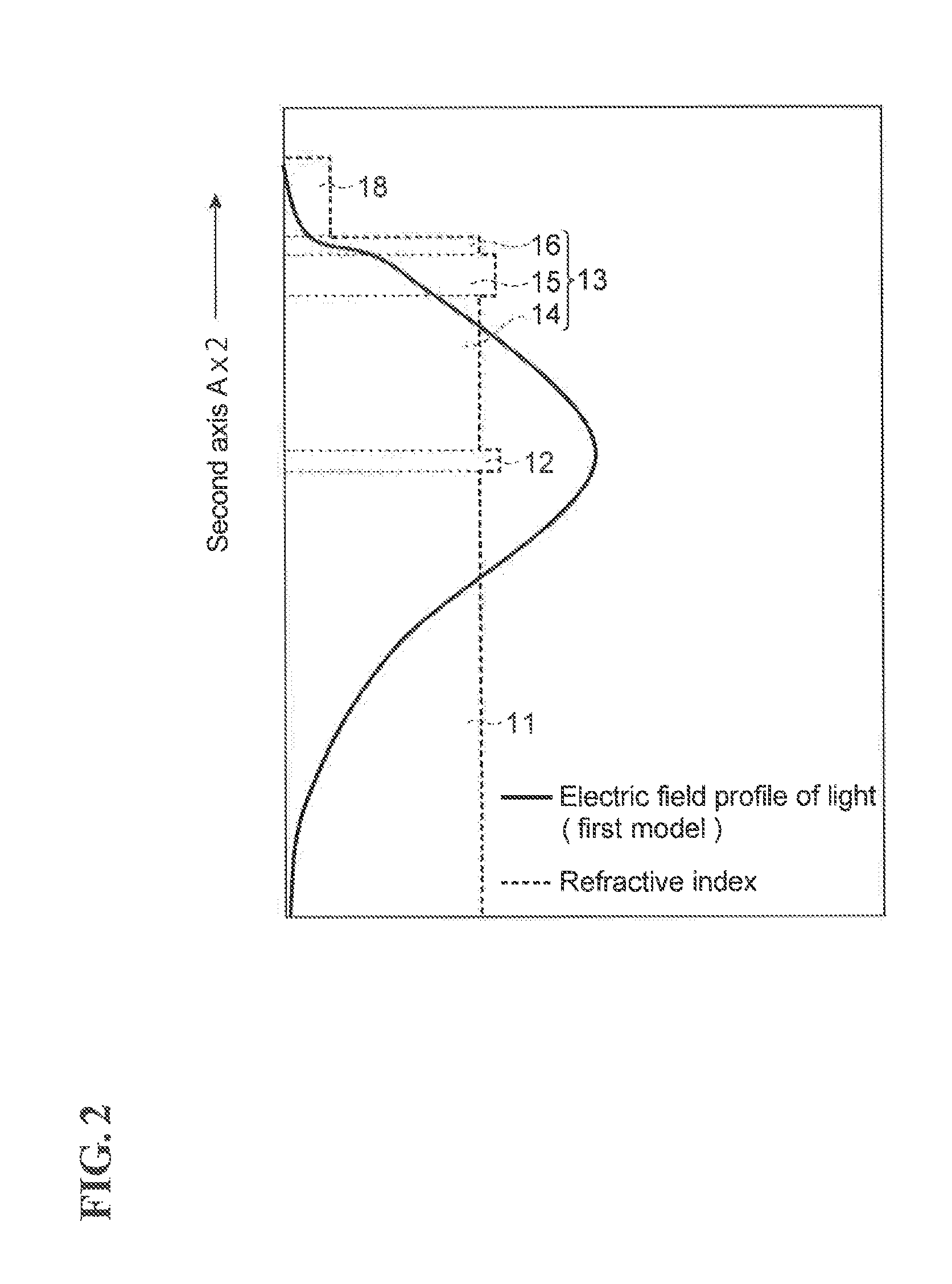
[0043]Referring to FIG. 1E, in the first optical waveguide 10, a cladding layer 13 includes a first cladding region 14, a semiconductor layer 15, and a second cladding region 16. The first cladding region 14, the semiconductor layer 15, and the second cladding region 16 are arranged in order in the direction of the second axis Ax2. The refractive index of the second cladding region 16 is equal to or lower than the refractive index of the first cladding region 14. The refractive index of a region 17 is lower than the refractive index of the second cladding region 16. The thickness of the second cladding region 16 is smaller than that of the first cladding region 14. The second cladding region 16 has a third surface 16A and a fourth surface 16B. The third surface 16A is located on the side opposite to the fourth surface 16B. In the preset embodiment, the second surface 15B of the semiconductor layer 15 is in contact with the third surface 16A of the second cladding...
example 4
Structural Example 4
[0045]Referring to FIG. 1F in the first optical waveguide 10, a cladding layer 13 includes a first cladding region 14, a semiconductor layer 15, and a second cladding region 16. The first cladding region 14, the semiconductor layer 15, and the second cladding region 16 are arranged in order in the direction of the second axis Ax2. An insulator layer 18 is disposed on the second cladding region 16 as a region 17. The cladding layer 13 is provided between the core layer 12 and the insulator layer 18. The insulator layer 18 is in contact with the cladding layer 13. A third surface 16A of the second cladding region 16 is in contact with a second surface 15B of the semiconductor layer 15. A fourth surface 16B of the second cladding region 16 is in contact with the insulator layer 18. The refractive index of the second cladding region 16 is equal to or lower than the refractive index of the first cladding region 14. The refractive index of the insulator layer 18 is low...
PUM
 Abstract
Description
Claims
Application Information
 - R&D
- Intellectual Property
- Life Sciences
- Materials
- Tech Scout
- Unparalleled Data Quality
- Higher Quality Content
- 60% Fewer Hallucinations
Browse by: Latest US Patents, China's latest patents, Technical Efficacy Thesaurus, Application Domain, Technology Topic, Popular Technical Reports.
© 2025 PatSnap. All rights reserved.Legal|Privacy policy|Modern Slavery Act Transparency Statement|Sitemap|About US| Contact US: help@patsnap.com